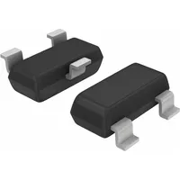
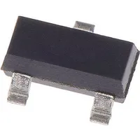
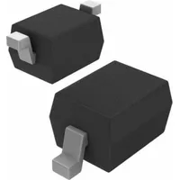
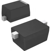
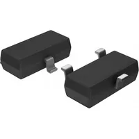
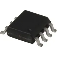
Infineon Technologies 2N7002DWH6327XTSA1
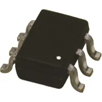
|
|
||||
|
|
Enhance your electronic projects with the high-quality 2N7002DWH6327XTSA1 Small Signal Field Effect Transistor from Infineon Technologies. With a focus on innovation and reliability, Infineon is a trusted manufacturer known for delivering top-notch components. This N-channel transistor is perfect for switching applications, offering a breakthrough in performance and efficiency. Its compact design, built-in diode, and low resistance make it a versatile choice for various projects. Trust in the value and benefits of this product to elevate your creations to new heights.
Package Body Material: PLASTIC/EPOXY
Provides durability and protection for the transistor, making it suitable for a variety of applications and environments.
Polarity or Channel Type: N-CHANNEL
Offers efficient and fast switching characteristics, ideal for many electronic circuits and applications.
Configuration: SEPARATE, 2 ELEMENTS WITH BUILT-IN DIODE
Allows for versatile usage in circuits requiring multiple elements with the added functionality of a built-in diode.
Transistor Application: SWITCHING
Designed specifically for switching applications, ensuring reliable performance in such scenarios.
Minimum DS Breakdown Voltage: 60 V
Offers a high breakdown voltage, providing an extra margin of safety in high voltage applications.
Surface Mount: YES
Enables easy and convenient mounting on circuit boards, saving space and simplifying assembly processes.
Field Effect Transistor Technology: METAL-OXIDE SEMICONDUCTOR
Features advanced MOSFET technology for efficient and high-performance transistor operation.
Maximum Drain Current (ID): 0.3 A
Can handle a maximum drain current of 0.3 A, suitable for various low-power applications.
Maximum Drain-Source On Resistance: 3 ohm
Provides low on-resistance for efficient power handling and reduced heat dissipation.
Maximum Feedback Capacitance (Crss): 3 pF
Low feedback capacitance helps in reducing signal distortion and improving overall circuit performance.
| Package Body Material: | PLASTIC/EPOXY |
| Configuration: | SEPARATE, 2 ELEMENTS WITH BUILT-IN DIODE |
| Transistor Element Material: | SILICON |
| Field Effect Transistor Technology: | METAL-OXIDE SEMICONDUCTOR |
| Transistor Application: | SWITCHING |
| Maximum Drain Current (ID): | .3 A |
| Surface Mount: | YES |
| Terminal Finish: | TIN |
| No. of Terminals: | 6 |
| Terminal Position: | DUAL |
| Package Style (Meter): | SMALL OUTLINE |
| JESD-30 Code: | R-PDSO-G6 |
| No. of Elements: | 2 |
| Package Shape: | RECTANGULAR |
| Terminal Form: | GULL WING |
| Operating Mode: | ENHANCEMENT MODE |
| Maximum Drain-Source On Resistance: | 3 ohm |
| Moisture Sensitivity Level (MSL): | 1 |
| Other Names: | 2832-2N7002DWH6327XTSA1<br>2N7002DWH6327XTSA1CT<br>2N7002DW H6327TR-ND<br>SP000917596<br>2N7002DW H6327DKR-ND<br>2N7002DW H6327-ND<br>2N7002DW H6327<br>2N7002DW H6327DKR<br>2N7002H6327XT<br>2N7002DWH6327XTSA1DKR<br>2N7002DW H6327CT-ND<br>2N7002DW H6327CT<br>2N7002DWH6327<br>2N7002DWH6327XTSA1TR |
| Maximum Feedback Capacitance (Crss): | 3 pF |
| Polarity or Channel Type: | N-CHANNEL |
| JESD-609 Code: | e3 |
| Minimum DS Breakdown Voltage: | 60 V |
| Qualification: | Not Qualified |
| Additional Features: | AVALANCHE RATED, LOGIC LEVEL COMPATIBLE |
| ECCN | EAR99 |
| ECCN Governance | EAR |
