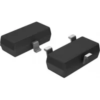
NXP Semiconductors BSS123,215

|
|
||||
|
|
Unlock the power of cutting-edge technology with the BSS123,215 by NXP Semiconductors. Designed for high-performance switching applications, this N-CHANNEL FET offers unparalleled reliability and efficiency. With a maximum operating temperature of 150°C and a minimum DS breakdown voltage of 100V, this transistor is built to withstand even the most demanding environments. Whether you're looking to enhance your electronic projects or streamline your industrial processes, the BSS123,215 delivers unmatched value and performance. Experience the difference with NXP Semiconductors today.
Package Body Material: PLASTIC/EPOXY
This material is lightweight and provides good heat dissipation, making the product durable and reliable for various applications.
Polarity or Channel Type: N-CHANNEL
N-channel FETs typically have higher mobility and conductivity, making them suitable for high-performance applications.
Configuration: SINGLE WITH BUILT-IN DIODE
The built-in diode simplifies circuit design and protects the transistor from reverse voltage spikes, enhancing overall performance.
Transistor Application: SWITCHING
Designed specifically for switching applications, ensuring fast and efficient operation in various electronic circuits.
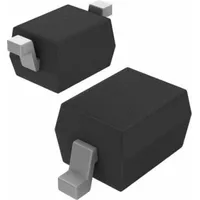
Surface Mount: YES
Easily mountable on PCBs, saving space and facilitating automated assembly processes.
Minimum DS Breakdown Voltage: 100 V
Can handle high voltage applications safely, providing reliable performance in demanding conditions.
Package Shape: RECTANGULAR
The rectangular shape allows for easy placement and alignment on circuit boards, optimizing space utilization.
Terminal Form: GULL WING
Gull wing terminals provide secure connections and ease of soldering during assembly, ensuring good electrical contact.
Operating Mode: ENHANCEMENT MODE
Enhancement mode FETs offer better control over the transistor's conductivity and enable precise switching operations.
Maximum Drain Current (Abs) (ID): 0.17 A
Capable of handling high currents, making it suitable for power switching applications.
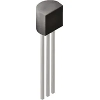
No. of Terminals: 3
The three terminals provide necessary connections for the FET to function effectively in a circuit.
Maximum Power Dissipation (Abs): 0.36 W
Can dissipate heat efficiently, ensuring stable operation under high power conditions.
Package Style (Meter): SMALL OUTLINE
Small outline package style saves space on PCBs and allows for high-density circuit designs.
Field Effect Transistor Technology: METAL-OXIDE SEMICONDUCTOR
Metal-oxide semiconductor technology offers good performance characteristics, such as low input capacitance and high switching speeds.
Maximum Operating Temperature: 150 °C
Can operate at high temperatures without performance degradation, suitable for industrial applications.
Transistor Element Material: SILICON
Silicon is a widely used semiconductor material known for its reliability and stability in electronic devices.
Terminal Finish: TIN
Tin terminal finish provides good solderability and corrosion resistance, enhancing the FET's reliability in different environments.
Maximum Drain-Source On Resistance: 6 ohm
Low on-resistance results in minimal power loss and improved efficiency in switching applications.
Terminal Position: DUAL
Dual terminal position offers flexibility in circuit design and allows for versatile connections in different applications.
Maximum Time At Peak Reflow Temperature (s): 30
Can withstand peak reflow temperatures for a specified duration during soldering processes without compromising its performance.
Peak Reflow Temperature °C: 260
Capable of withstanding high reflow temperatures during assembly processes, ensuring reliability in manufacturing.
Maximum Feedback Capacitance (Crss): 10 pF
Low feedback capacitance results in minimal signal distortion and improved high-frequency performance in amplifying circuits.
| Package Body Material: | PLASTIC/EPOXY |
| Maximum Time At Peak Reflow Temperature (s): | 30 |
| Configuration: | SINGLE WITH BUILT-IN DIODE |
| Transistor Element Material: | SILICON |
| Field Effect Transistor Technology: | METAL-OXIDE SEMICONDUCTOR |
| Transistor Application: | SWITCHING |
| Maximum Drain Current (ID): | .15 A |
| Sub-Category: | FET General Purpose Powers |
| Surface Mount: | YES |
| Terminal Finish: | TIN |
| No. of Terminals: | 3 |
| Maximum Power Dissipation (Abs): | .36 W |
| Terminal Position: | DUAL |
| Package Style (Meter): | SMALL OUTLINE |
| JESD-30 Code: | R-PDSO-G3 |
| No. of Elements: | 1 |
| Package Shape: | RECTANGULAR |
| Terminal Form: | GULL WING |
| Operating Mode: | ENHANCEMENT MODE |
| Maximum Operating Temperature: | 150 Cel |
| Maximum Drain-Source On Resistance: | 6 ohm |
| Moisture Sensitivity Level (MSL): | 1 |
| Maximum Feedback Capacitance (Crss): | 10 pF |
| Polarity or Channel Type: | N-CHANNEL |
| JESD-609 Code: | e3 |
| Minimum DS Breakdown Voltage: | 100 V |
| Qualification: | Not Qualified |
| Maximum Drain Current (Abs) (ID): | .17 A |
| Peak Reflow Temperature (C): | 260 |
| ECCN | EAR99 |
| ECCN Governance | EAR |
| HTS | 8541.21.00.95 |
| SB | 8541.21.00.80 |

