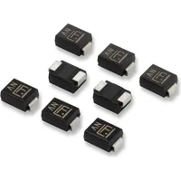
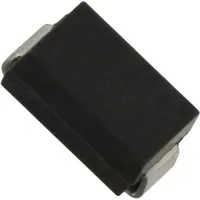
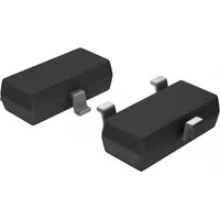
Diodes Incorporated BSS138-7-F
|
|
||||
|
|
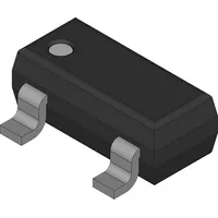
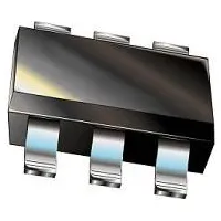
Discover the BSS138-7-F by Diodes Incorporated, a top-quality small signal field effect transistor designed for switching applications. With its N-channel polarity and built-in diode configuration, this transistor offers superior performance and reliability. Perfect for surface mount applications, this enhancement mode transistor boasts a maximum drain current of 0.2A and a minimum DS breakdown voltage of 50V. Trust in the expertise of Diodes Incorporated to provide you with cutting-edge technology that delivers exceptional value and efficiency. Elevate your electronic projects with the BSS138-7-F and experience the difference today.
Package Body Material: PLASTIC/EPOXY
Provides durability and protection for the internal components of the transistor.
Polarity or Channel Type: N-CHANNEL
N-channel transistors typically offer higher mobility and faster switching speeds compared to P-channel transistors.
Configuration: SINGLE WITH BUILT-IN DIODE
The built-in diode allows for efficient switching and protection against reverse current flow.
Transistor Application: SWITCHING
Designed for fast and efficient switching applications.
Minimum DS Breakdown Voltage: 50 V
Can withstand high voltages, making it suitable for a variety of voltage applications.
Surface Mount: YES
Easily mountable on circuit boards, saving space and simplifying assembly.
Maximum Drain Current (Abs) (ID): 0.2 A
Able to handle a current of 0.2 A, suitable for low-power applications.
Maximum Power Dissipation (Abs): 0.3 W
Withstands power dissipation of up to 0.3 W, ensuring reliable performance under load.
Maximum Operating Temperature: 150 °C
Operates effectively at high temperatures, providing versatility in various environments.
Maximum Drain-Source On Resistance: 3.5 ohm
Low on-resistance allows for efficient conduction and minimal power loss.
| Package Body Material: | PLASTIC/EPOXY |
| Maximum Time At Peak Reflow Temperature (s): | 30 |
| Configuration: | SINGLE WITH BUILT-IN DIODE |
| Transistor Element Material: | SILICON |
| Field Effect Transistor Technology: | METAL-OXIDE SEMICONDUCTOR |
| Transistor Application: | SWITCHING |
| Maximum Drain Current (ID): | .2 A |
| Sub-Category: | FET General Purpose Powers |
| Surface Mount: | YES |
| Terminal Finish: | MATTE TIN |
| No. of Terminals: | 3 |
| Maximum Power Dissipation (Abs): | .3 W |
| Terminal Position: | DUAL |
| Package Style (Meter): | SMALL OUTLINE |
| JESD-30 Code: | R-PDSO-G3 |
| No. of Elements: | 1 |
| Package Shape: | RECTANGULAR |
| Terminal Form: | GULL WING |
| Operating Mode: | ENHANCEMENT MODE |
| Maximum Operating Temperature: | 150 Cel |
| Maximum Drain-Source On Resistance: | 3.5 ohm |
| Moisture Sensitivity Level (MSL): | 1 |
| Maximum Feedback Capacitance (Crss): | 8 pF |
| Polarity or Channel Type: | N-CHANNEL |
| JESD-609 Code: | e3 |
| Minimum DS Breakdown Voltage: | 50 V |
| Qualification: | Not Qualified |
| Additional Features: | HIGH RELIABILITY, LOW THRESHOLD |
| Maximum Drain Current (Abs) (ID): | .2 A |
| Peak Reflow Temperature (C): | 260 |
| ECCN | EAR99 |
| ECCN Governance | EAR |
