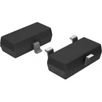
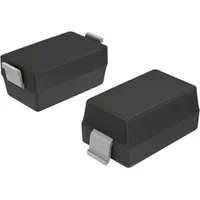
Onsemi FDN306P

|
|
||||
|
|
Unlock the power of small signal field effect transistors with the FDN306P by Onsemi. Manufactured by a trusted industry leader, this P-channel transistor with a built-in diode offers reliable switching capabilities for a wide range of applications. Its high-quality construction and advanced technology ensure optimal performance, while its compact design makes it perfect for space-saving solutions. Trust Onsemi to deliver value, benefits, and advantages that go beyond expectations with the FDN306P - the ultimate choice for your next project.
Package Body Material: PLASTIC/EPOXY
PLASTIC/EPOXY material is commonly used for packaging as it provides good insulation and protection for the transistor, ensuring reliable performance.
Polarity or Channel Type: P-CHANNEL
P-CHANNEL type is suitable for switching applications and can provide better performance in certain circuits compared to N-CHANNEL transistors.
Configuration: SINGLE WITH BUILT-IN DIODE
Having a built-in diode can simplify circuit design and provide additional functionality without the need for external components.
Transistor Application: SWITCHING
Designed specifically for switching applications, this transistor can efficiently and effectively control the flow of current in a circuit.
Maximum Drain Current (ID): 2.6 A
With a high maximum drain current rating, this transistor can handle higher current loads, making it suitable for a variety of applications.
Maximum Drain-Source On Resistance: 0.04 ohm
Low on-resistance results in minimal power loss and improved efficiency in the circuit, making this transistor an excellent choice for high-performance applications.
| Package Body Material: | PLASTIC/EPOXY |
| Maximum Time At Peak Reflow Temperature (s): | 30 |
| Configuration: | SINGLE WITH BUILT-IN DIODE |
| Transistor Element Material: | SILICON |
| Field Effect Transistor Technology: | METAL-OXIDE SEMICONDUCTOR |
| Transistor Application: | SWITCHING |
| Maximum Drain Current (ID): | 2.6 A |
| Surface Mount: | YES |
| Terminal Finish: | MATTE TIN |
| No. of Terminals: | 3 |
| Maximum Power Dissipation (Abs): | .5 W |
| Terminal Position: | DUAL |
| Package Style (Meter): | SMALL OUTLINE |
| JESD-30 Code: | R-PDSO-G3 |
| No. of Elements: | 1 |
| Package Shape: | RECTANGULAR |
| Terminal Form: | GULL WING |
| Operating Mode: | ENHANCEMENT MODE |
| Maximum Operating Temperature: | 150 Cel |
| Maximum Power Dissipation Ambient: | .5 W |
| Maximum Drain-Source On Resistance: | .04 ohm |
| Moisture Sensitivity Level (MSL): | 1 |
| Polarity or Channel Type: | P-CHANNEL |
| JESD-609 Code: | e3 |
| Minimum Operating Temperature: | -55 Cel |
| Minimum DS Breakdown Voltage: | 12 V |
| Qualification: | Not Qualified |
| Peak Reflow Temperature (C): | 260 |
| ECCN | EAR99 |
| ECCN Governance | EAR |
| HTS | 8541.21.00.95 |
| SB | 8541.21.00.80 |
