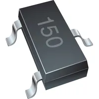
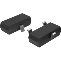
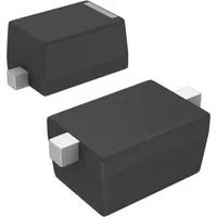
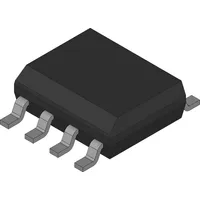
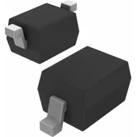
Infineon Technologies BSS138NH6327XTSA2
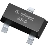
|
|
||||
|
|
Unlock the power of cutting-edge technology with the BSS138NH6327XTSA2 by Infineon Technologies. As a leader in the industry, Infineon guarantees top-quality manufacturing and innovation. This Small Signal Field Effect Transistor (FET) is designed for enhanced performance and reliability. With its N-CHANNEL polarity and built-in diode, this transistor offers incredible value and versatility. Perfect for a wide range of applications, this product is sure to exceed your expectations. Trust Infineon for superior quality and unmatched benefits that will elevate your projects to new heights.
Package Body Material: PLASTIC/EPOXY
This material provides good protection against external elements and ensures durability.
Polarity or Channel Type: N-CHANNEL
N-channel transistors typically have better performance and efficiency compared to P-channel transistors.
Surface Mount: YES
Allows for easy and compact integration onto circuit boards.
Minimum DS Breakdown Voltage: 60 V
Suitable for applications requiring higher voltage handling capabilities.
Operating Mode: ENHANCEMENT MODE
Enhancement mode transistors offer better control and faster response times.
Maximum Power Dissipation (Abs): 0.36 W
Can handle moderate power levels without overheating.
Maximum Operating Temperature: 150 °C
Can operate efficiently even in high temperature environments.
Maximum Drain-Source On Resistance: 3.5 ohm
Low on-resistance ensures minimal power loss and high efficiency.
Maximum Drain Current (ID): 0.23 A
Able to handle a decent amount of current flow.
Maximum Feedback Capacitance (Crss): 3.8 pF
Low feedback capacitance helps in reducing signal distortion.
| Package Body Material: | PLASTIC/EPOXY |
| Maximum Time At Peak Reflow Temperature (s): | 30 |
| Configuration: | SINGLE WITH BUILT-IN DIODE |
| Transistor Element Material: | SILICON |
| Field Effect Transistor Technology: | METAL-OXIDE SEMICONDUCTOR |
| Maximum Drain Current (ID): | .23 A |
| Surface Mount: | YES |
| Terminal Finish: | TIN |
| No. of Terminals: | 3 |
| Maximum Power Dissipation (Abs): | .36 W |
| Terminal Position: | DUAL |
| Package Style (Meter): | SMALL OUTLINE |
| JESD-30 Code: | R-PDSO-G3 |
| No. of Elements: | 1 |
| Package Shape: | RECTANGULAR |
| Terminal Form: | GULL WING |
| Operating Mode: | ENHANCEMENT MODE |
| Maximum Operating Temperature: | 150 Cel |
| Maximum Power Dissipation Ambient: | .36 W |
| Maximum Drain-Source On Resistance: | 3.5 ohm |
| Moisture Sensitivity Level (MSL): | 1 |
| Other Names: | BSS138NH6327XTSA1<br>SP000919330<br>BSS138N H6327-ND<br>BSS138NH6327XTSA2DKR<br>BSS138NH6327XTSA2CT<br>BSS138NH6327XTSA2INACTIVE<br>BSS138NH6327XTSA2TR<br>BSS138NH6327XTSA2-ND<br>BSS138N H6327<br>SP000639080 |
| Maximum Feedback Capacitance (Crss): | 3.8 pF |
| Polarity or Channel Type: | N-CHANNEL |
| JESD-609 Code: | e3 |
| Minimum Operating Temperature: | -55 Cel |
| Minimum DS Breakdown Voltage: | 60 V |
| Additional Features: | LOGIC LEVEL COMPATIBLE |
| Reference Standard: | AEC-Q101; IEC-61249-2-21 |
| Peak Reflow Temperature (C): | 260 |
| ECCN | EAR99 |
| ECCN Governance | EAR |
| HTS | 8541.21.00.95 |
| SB | 8541.21.00.80 |

