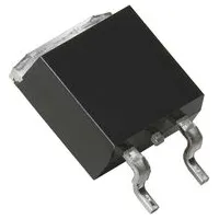
Onsemi FDD5614P
|
|
||||
|
|
Discover the FDD5614P by Onsemi, a high-quality Power Field Effect Transistor designed for switching applications. With its P-Channel configuration and built-in diode, this transistor offers unmatched efficiency and reliability. Whether you're looking to optimize power management in automotive, industrial, or consumer electronics, the FDD5614P delivers exceptional performance with a maximum drain current of 15A and low on-resistance. Trust Onsemi's expertise in semiconductor technology to bring you cutting-edge solutions that enhance your products' capabilities. Upgrade your designs today with the FDD5614P.
Package Body Material: PLASTIC/EPOXY
The use of plastic/epoxy material makes this FET lightweight and durable, ideal for portable and rugged applications.
Polarity or Channel Type: P-CHANNEL
P-channel FETs offer low on-resistance and high current-carrying capabilities, making them efficient for power management applications.
Configuration: SINGLE WITH BUILT-IN DIODE
The built-in diode simplifies circuit design and protects against back EMF, offering added convenience and reliability.
Transistor Application: SWITCHING
Designed specifically for switching applications, this FET provides fast and efficient control over power flow in a circuit.
Surface Mount: YES
The surface mount capability allows for easy and compact PCB assembly, saving space and reducing overall system size.
Minimum DS Breakdown Voltage: 60 V
With a high breakdown voltage, this FET can handle higher voltage levels without the risk of damage, ensuring safe and reliable operation.
Package Shape: RECTANGULAR
The rectangular shape of the package offers versatility in mounting options and compatibility with various layouts, enhancing ease of installation.
Terminal Form: GULL WING
The gull wing terminal form provides secure and reliable connections, reducing the risk of signal loss or disconnection.
Operating Mode: ENHANCEMENT MODE
Enhancement mode operation allows for easy control of the FET's conductivity, enabling precise and efficient power management.
Maximum Pulsed Drain Current (IDM): 45 A
With a high pulsed drain current rating, this FET can handle sudden spikes in current without the risk of overheating or failure.
| Package Body Material: | PLASTIC/EPOXY |
| Maximum Time At Peak Reflow Temperature (s): | 30 |
| Configuration: | SINGLE WITH BUILT-IN DIODE |
| Transistor Element Material: | SILICON |
| Field Effect Transistor Technology: | METAL-OXIDE SEMICONDUCTOR |
| Transistor Application: | SWITCHING |
| Maximum Drain Current (ID): | 15 A |
| Maximum Pulsed Drain Current (IDM): | 45 A |
| Sub-Category: | Other Transistors |
| Surface Mount: | YES |
| Terminal Finish: | MATTE TIN |
| No. of Terminals: | 2 |
| Maximum Power Dissipation (Abs): | 42 W |
| Terminal Position: | SINGLE |
| Package Style (Meter): | SMALL OUTLINE |
| JESD-30 Code: | R-PSSO-G2 |
| No. of Elements: | 1 |
| Package Shape: | RECTANGULAR |
| Terminal Form: | GULL WING |
| Operating Mode: | ENHANCEMENT MODE |
| Maximum Operating Temperature: | 175 Cel |
| Case Connection: | DRAIN |
| Maximum Drain-Source On Resistance: | .1 ohm |
| Moisture Sensitivity Level (MSL): | 1 |
| Avalanche Energy Rating (EAS): | 90 mJ |
| JEDEC-95 Code: | TO-252 |
| Polarity or Channel Type: | P-CHANNEL |
| JESD-609 Code: | e3 |
| Minimum DS Breakdown Voltage: | 60 V |
| Qualification: | Not Qualified |
| Maximum Drain Current (Abs) (ID): | 15 A |
| Peak Reflow Temperature (C): | 260 |
| ECCN | EAR99 |
| ECCN Governance | EAR |
