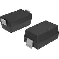
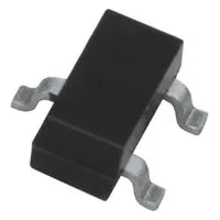
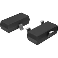
NXP Semiconductors BSS138PS,115
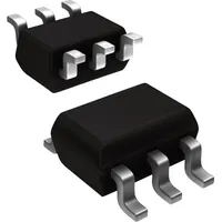
|
|
||||
|
|
Discover the power of the BSS138PS,115 by NXP Semiconductors, a top-quality N-CHANNEL Small Signal Field Effect Transistor (FET) perfect for switching applications. With a robust design and built-in diode, this transistor offers reliability and efficiency like no other. Whether you're looking to enhance your electronic projects or streamline your manufacturing processes, the BSS138PS,115 delivers unmatched performance and value. Upgrade your devices with this cutting-edge technology and experience the difference today.
Package Body Material: PLASTIC/EPOXY
The plastic/epoxy material makes the transistor lightweight and durable, suitable for various applications.
Polarity or Channel Type: N-CHANNEL
N-Channel transistors typically have better conductivity and lower resistance, making them efficient for switching applications.
Transistor Application: SWITCHING
Designed specifically for switching applications, ensuring reliable performance in on/off states.
Minimum DS Breakdown Voltage: 60 V
With a minimum breakdown voltage of 60 V, this transistor can handle higher voltages, adding to its versatility.
Surface Mount: YES
Surface mount capability allows for easy and convenient installation on circuit boards, saving space and simplifying assembly processes.
Maximum Drain Current (ID): 0.32 A
With a maximum drain current of 0.32 A, this transistor can handle moderate current loads with efficiency.
Maximum Drain-Source On Resistance: 1.6 ohm
Low drain-source resistance of 1.6 ohm ensures minimal power loss and efficient performance in switching applications.
| Package Body Material: | PLASTIC/EPOXY |
| Maximum Time At Peak Reflow Temperature (s): | 30 |
| Configuration: | SEPARATE, 2 ELEMENTS WITH BUILT-IN DIODE |
| Transistor Element Material: | SILICON |
| Field Effect Transistor Technology: | METAL-OXIDE SEMICONDUCTOR |
| Transistor Application: | SWITCHING |
| Maximum Drain Current (ID): | .32 A |
| Surface Mount: | YES |
| Terminal Finish: | TIN |
| No. of Terminals: | 6 |
| Terminal Position: | DUAL |
| Package Style (Meter): | SMALL OUTLINE |
| JESD-30 Code: | R-PDSO-G6 |
| No. of Elements: | 2 |
| Package Shape: | RECTANGULAR |
| Terminal Form: | GULL WING |
| Operating Mode: | ENHANCEMENT MODE |
| Maximum Drain-Source On Resistance: | 1.6 ohm |
| Moisture Sensitivity Level (MSL): | 1 |
| Polarity or Channel Type: | N-CHANNEL |
| JESD-609 Code: | e3 |
| Minimum DS Breakdown Voltage: | 60 V |
| Additional Features: | LOGIC LEVEL COMPATIBLE |
| Reference Standard: | AEC-Q101 |
| Peak Reflow Temperature (C): | 260 |
| ECCN | EAR99 |
| ECCN Governance | EAR |
