| Package Body Material: |
PLASTIC/EPOXY |
| Maximum Time At Peak Reflow Temperature (s): |
30 |
| Configuration: |
SINGLE WITH BUILT-IN DIODE |
| Transistor Element Material: |
SILICON |
| Field Effect Transistor Technology: |
METAL-OXIDE SEMICONDUCTOR |
| Transistor Application: |
SWITCHING |
| Maximum Drain Current (ID): |
3 A |
| Sub-Category: |
Other Transistors |
| Surface Mount: |
YES |
| Terminal Finish: |
MATTE TIN |
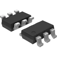
| No. of Terminals: |
6 |
| Maximum Power Dissipation (Abs): |
1.6 W |
| Terminal Position: |
DUAL |
| Package Style (Meter): |
SMALL OUTLINE |
| JESD-30 Code: |
R-PDSO-G6 |
| No. of Elements: |
1 |
| Package Shape: |
RECTANGULAR |
| Terminal Form: |
GULL WING |
| Operating Mode: |
ENHANCEMENT MODE |
| Maximum Operating Temperature: |
150 Cel |
| Maximum Drain-Source On Resistance: |
.105 ohm |
| Moisture Sensitivity Level (MSL): |
1 |
| Other Names: |
FDC5614PCT<br>FDC5614PDKR<br>FDC5614PTR |
| Polarity or Channel Type: |
P-CHANNEL |
| JESD-609 Code: |
e3 |
| Minimum DS Breakdown Voltage: |
60 V |
| Qualification: |
Not Qualified |
| Maximum Drain Current (Abs) (ID): |
3 A |
| Peak Reflow Temperature (C): |
260 |
