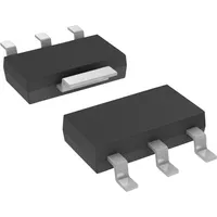
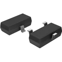
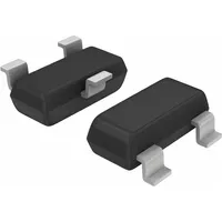
NXP Semiconductors BSS138BK,215
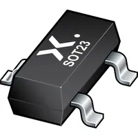
|
|
||||
|
|
Discover the power of the BSS138BK,215 by NXP Semiconductors, a high-quality Power FET that delivers unmatched performance and reliability. With its N-CHANNEL configuration and ENHANCEMENT MODE operation, this transistor is perfect for a wide range of applications. From consumer electronics to industrial automation, this versatile component offers exceptional value and benefits to customers seeking cutting-edge technology. Trust NXP Semiconductors for innovative solutions that exceed expectations.
Polarity or Channel Type: N-CHANNEL
N-CHANNEL FETs are commonly used in power applications due to their high efficiency and low ON-state resistance.
Configuration: SINGLE
Single configuration FETs are easy to use and implement in circuits, making the product suitable for various applications.
Surface Mount: YES
Surface mount capability allows for easy and efficient PCB assembly, saving time and labor costs.
Operating Mode: ENHANCEMENT MODE
Enhancement mode FETs offer better control over the device's operation and can be used in a wider range of applications.
Maximum Drain Current (Abs): 0.36 A
With a high maximum drain current, this FET can handle various power requirements in different applications.
Maximum Power Dissipation (Abs): 0.42 W
Efficient power dissipation ensures the FET can operate within its limits without overheating, enhancing its reliability.
Field Effect Transistor Technology: METAL-OXIDE SEMICONDUCTOR
Metal-oxide semiconductor technology offers high performance, reliability, and efficiency in power applications.
Maximum Operating Temperature: 150 °C
With a high maximum operating temperature, this FET can withstand harsh environments and operate reliably under varying conditions.
Terminal Finish: TIN
Tin terminal finish provides good solderability and corrosion resistance, ensuring reliable connections in circuit assemblies.
Maximum Time At Peak Reflow Temperature (s): 30
Short time at peak reflow temperature during assembly minimizes thermal stress on the device and improves overall solder joint quality.
Peak Reflow Temperature °C: 260
High peak reflow temperature capability ensures proper soldering and rework processes, leading to better product quality and reliability.
| Maximum Time At Peak Reflow Temperature (s): | 30 |
| Configuration: | SINGLE |
| Field Effect Transistor Technology: | METAL-OXIDE SEMICONDUCTOR |
| Maximum Drain Current (ID): | .36 A |
| Sub-Category: | FET General Purpose Power |
| Polarity or Channel Type: | N-CHANNEL |
| Surface Mount: | YES |
| Terminal Finish: | TIN |
| JESD-609 Code: | e3 |
| Maximum Power Dissipation (Abs): | .42 W |
| No. of Elements: | 1 |
| Operating Mode: | ENHANCEMENT MODE |
| Maximum Operating Temperature: | 150 Cel |
| Maximum Drain Current (Abs) (ID): | .36 A |
| Peak Reflow Temperature (C): | 260 |
| Moisture Sensitivity Level (MSL): | 1 |
| ECCN | EAR99 |
| ECCN Governance | EAR |
