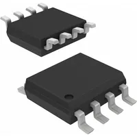
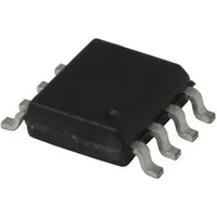
Onsemi NDT2955
|
|
||||
|
|
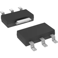
Discover the power of innovation with the NDT2955 by Onsemi. As a leading manufacturer in the field of Power Field Effect Transistors, Onsemi delivers top-notch quality and reliability. The NDT2955, with its P-CHANNEL polarity and SINGLE configuration, is ideal for various switching applications. With a maximum pulsing drain current of 15 A and a low on-resistance of 0.3 ohm, this transistor offers exceptional performance and efficiency. Whether you're looking to optimize your power management system or enhance your electronic devices, the NDT2955 provides the value and benefits that customers need. Trust Onsemi to deliver cutting-edge technology that meets your needs.
Package Body Material: PLASTIC/EPOXY
Provides durability and protection for the internal components, ensuring a long lifespan for the product.
Polarity or Channel Type: P-CHANNEL
Allows for efficient control and switching of power flow in electronic circuits.
Configuration: SINGLE WITH BUILT-IN DIODE
Simplifies circuit design by integrating a diode, saving space and reducing component count.
Transistor Application: SWITCHING
Designed specifically for switching applications, ensuring reliable performance in power control systems.
Surface Mount: YES
Enables easy and efficient mounting on circuit boards, saving assembly time and reducing overall product size.
Minimum DS Breakdown Voltage: 60 V
Allows for operation in high voltage environments, making the product suitable for a wide range of applications.
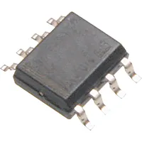
Package Shape: RECTANGULAR
Compact shape facilitates easy integration into circuit designs and saves space in electronic systems.
Terminal Form: GULL WING
Provides secure and reliable solder connections, ensuring stable electrical connections in the circuit.
Operating Mode: ENHANCEMENT MODE
Enhancement mode operation offers precise control over power flow, improving the efficiency of the switching process.
Maximum Pulsed Drain Current (IDM): 15 A
Capable of handling high current surges, making it suitable for demanding power control applications.
Avalanche Energy Rating (EAS): 174 mJ
Provides protection against voltage spikes and surges, enhancing the reliability of the product in harsh operating conditions.
Maximum Drain Current (Abs) (ID): 2.5 A
Can deliver a steady current flow, ensuring stable operation in various power control scenarios.
Maximum Power Dissipation (Abs): 3 W
Efficiently dissipates heat generated during operation, preventing overheating and ensuring long-term reliability.
| Package Body Material: | PLASTIC/EPOXY |
| Maximum Time At Peak Reflow Temperature (s): | 30 |
| Configuration: | SINGLE WITH BUILT-IN DIODE |
| Transistor Element Material: | SILICON |
| Field Effect Transistor Technology: | METAL-OXIDE SEMICONDUCTOR |
| Transistor Application: | SWITCHING |
| Maximum Drain Current (ID): | 2.5 A |
| Maximum Pulsed Drain Current (IDM): | 15 A |
| Sub-Category: | Other Transistors |
| Surface Mount: | YES |
| Terminal Finish: | MATTE TIN |
| No. of Terminals: | 4 |
| Maximum Power Dissipation (Abs): | 3 W |
| Terminal Position: | DUAL |
| Package Style (Meter): | SMALL OUTLINE |
| JESD-30 Code: | R-PDSO-G4 |
| No. of Elements: | 1 |
| Package Shape: | RECTANGULAR |
| Terminal Form: | GULL WING |
| Operating Mode: | ENHANCEMENT MODE |
| Maximum Operating Temperature: | 150 Cel |
| Case Connection: | DRAIN |
| Maximum Drain-Source On Resistance: | .3 ohm |
| Moisture Sensitivity Level (MSL): | 1 |
| Avalanche Energy Rating (EAS): | 174 mJ |
| Polarity or Channel Type: | P-CHANNEL |
| JESD-609 Code: | e3 |
| Minimum Operating Temperature: | -55 Cel |
| Minimum DS Breakdown Voltage: | 60 V |
| Qualification: | Not Qualified |
| Maximum Drain Current (Abs) (ID): | 2.5 A |
| Peak Reflow Temperature (C): | 260 |
| ECCN | EAR99 |
| ECCN Governance | EAR |
| NSN | 5961-01-609-8434, 5961016098434 |
| NIIN | 016098434 |

