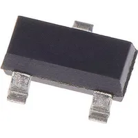
Diodes Incorporated MMBT3904-7-F
|
|
||||
|
|
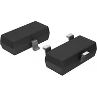
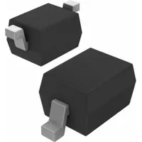
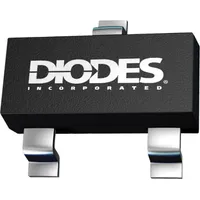
Looking for a reliable small signal bipolar junction transistor? Look no further than the MMBT3904-7-F by Diodes Incorporated. With a maximum VCEsat of only 0.3V and a minimum DC current gain of 30, this NPN transistor is perfect for switching applications. Its surface mount design and maximum operating temperature of 150°C make it versatile and durable. Trust in the quality of Diodes Incorporated and experience the value and benefits that the MMBT3904-7-F brings to your electronic projects.
Package Body Material: PLASTIC/EPOXY
This material offers durability and robustness, making the product suitable for various applications.
Polarity or Channel Type: NPN
NPN configuration allows for efficient amplification and switching capabilities in circuits.
Configuration: SINGLE
Single configuration simplifies circuit design and reduces complexity in applications.
Transistor Application: SWITCHING
Designed specifically for switching applications, ensuring reliable performance in high-speed operations.
Surface Mount: YES
Surface mount capability allows for easy installation on PCBs, saving space and improving overall system efficiency.
Maximum VCEsat: 0.3 V
Low VCE saturation voltage minimizes power loss and enhances overall energy efficiency of the circuit.
Package Shape: RECTANGULAR
Rectangular shape facilitates easy integration into various electronic systems and designs.
Terminal Form: GULL WING
Gull wing terminals offer secure connections and ease of soldering during assembly.
No. of Terminals: 3
Three terminals provide simple connectivity options and compatibility with common circuit configurations.
Maximum Power Dissipation (Abs): 0.35 W
High power dissipation rating allows for reliable operation under heavy loads and in demanding conditions.
Package Style (Meter): SMALL OUTLINE
Small outline package style saves space and allows for high-density PCB layouts.
Minimum DC Current Gain (hFE): 30
High DC current gain ensures stable and consistent amplification performance in various circuit configurations.
Maximum Operating Temperature: 150 °C
High operating temperature range allows for versatility in different environmental conditions.
Maximum Collector-Base Capacitance: 4 pF
Low collector-base capacitance minimizes signal distortion and improves high-frequency performance.
Maximum Collector-Emitter Voltage: 40 V
High collector-emitter voltage rating provides a wide voltage range for various applications.
Transistor Element Material: SILICON
Silicon material offers high reliability and stability for long-term operation.
Maximum Turn On Time (ton): 70 ns
Fast turn-on time ensures quick response and high-speed switching capabilities.
Minimum Operating Temperature: -55 °C
Wide operating temperature range allows for reliable performance in extreme conditions.
Maximum Collector Current (IC): 0.2 A
Maximum collector current ensures efficient handling of high currents in circuit applications.
Maximum Turn Off Time (toff): 250 ns
Fast turn-off time enhances switching speed and efficiency in dynamic circuit operations.
Terminal Finish: MATTE TIN
Matte tin finish provides corrosion resistance and solderability for reliable connections.
Terminal Position: DUAL
Dual terminal position offers flexibility in circuit design and layout.
Maximum Time At Peak Reflow Temperature (s): 30
Short reflow time at peak temperature ensures reliable solder joints and component integrity.
Peak Reflow Temperature °C: 260
High peak reflow temperature tolerance allows for robust assembly processes and compatibility with industry standards.
Reference Standard: AEC-Q101
Compliance with AEC-Q101 standards ensures high quality and reliability for automotive applications.
Nominal Transition Frequency (fT): 300 MHz
High transition frequency enables high-speed operation and improved performance in RF applications.
| Nominal Transition Frequency (fT): | 300 MHz |
| Package Body Material: | PLASTIC/EPOXY |
| Maximum Collector Current (IC): | .2 A |
| Maximum Time At Peak Reflow Temperature (s): | 30 |
| Configuration: | SINGLE |
| Transistor Element Material: | SILICON |
| Transistor Application: | SWITCHING |
| Maximum Turn On Time (ton): | 70 ns |
| Surface Mount: | YES |
| Terminal Finish: | MATTE TIN |
| No. of Terminals: | 3 |
| Maximum Power Dissipation (Abs): | .35 W |
| Terminal Position: | DUAL |
| Package Style (Meter): | SMALL OUTLINE |
| Maximum Turn Off Time (toff): | 250 ns |
| JESD-30 Code: | R-PDSO-G3 |
| No. of Elements: | 1 |
| Package Shape: | RECTANGULAR |
| Terminal Form: | GULL WING |
| Maximum Operating Temperature: | 150 Cel |
| Moisture Sensitivity Level (MSL): | 1 |
| Other Names: | MMBT3904-FDITR<br>MMBT39047F<br>MMBT3904-FDICT<br>MMBT3904-FDIDKR |
| Polarity or Channel Type: | NPN |
| Minimum DC Current Gain (hFE): | 30 |
| JESD-609 Code: | e3 |
| Minimum Operating Temperature: | -55 Cel |
| Qualification: | Not Qualified |
| Maximum Collector-Emitter Voltage: | 40 V |
| Additional Features: | HIGH RELIABILITY |
| Maximum Collector-Base Capacitance: | 4 pF |
| Reference Standard: | AEC-Q101 |
| Peak Reflow Temperature (C): | 260 |
| Maximum VCEsat: | .3 V |
| ECCN | EAR99 |
| ECCN Governance | EAR |
