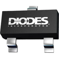
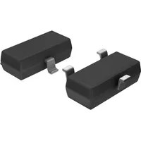
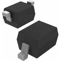
Infineon Technologies BSS84PH6327XTSA2
|
|
||||
|
|
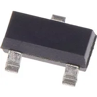
Discover the power of Infineon Technologies with the BSS84PH6327XTSA2, a high-quality P-CHANNEL FET perfect for switching applications. With its innovative design and reliable performance, this transistor offers customers unmatched value and efficiency. Whether you're looking to improve your electronic devices or enhance your projects, the BSS84PH6327XTSA2 delivers on all fronts. Trust in Infineon Technologies to provide cutting-edge solutions that exceed expectations.
Package Body Material: PLASTIC/EPOXY
This material is lightweight and durable, making the product suitable for portable devices.
Polarity or Channel Type: P-CHANNEL
P-channel FETs are known for their low gate leakage and high input impedance, ensuring efficient switching performance.
Configuration: SINGLE WITH BUILT-IN DIODE
The built-in diode allows for reverse bias protection, making the product versatile and reliable.
Transistor Application: SWITCHING
Designed specifically for switching applications, ensuring fast and efficient operation.
Surface Mount: YES
Surface mount packaging allows for easy integration onto PCBs, saving space and simplifying assembly.
Minimum DS Breakdown Voltage: 60 V
The high breakdown voltage provides a safety margin for voltage spikes, increasing reliability.
Package Shape: RECTANGULAR
Rectangular shape facilitates easy placement and alignment on a circuit board.
Terminal Form: GULL WING
Gull-wing terminals are suitable for surface mount soldering, ensuring secure connections.
Operating Mode: ENHANCEMENT MODE
Enhancement mode FETs offer high input resistance and low conduction resistance, improving efficiency.
Maximum Drain Current (Abs) (ID): 0.17 A
The high maximum drain current allows for handling of higher power loads.
No. of Terminals: 3
With three terminals, the FET can be easily configured in various circuit designs.
Maximum Power Dissipation (Abs): 0.36 W
The low power dissipation rating indicates the FET can operate efficiently without overheating.
Package Style (Meter): SMALL OUTLINE
The small outline package saves space on the PCB, ideal for compact electronic devices.
Field Effect Transistor Technology: METAL-OXIDE SEMICONDUCTOR
MOSFET technology ensures high switching speeds and low power consumption for improved performance.
Maximum Operating Temperature: 150 °C
The high maximum operating temperature range allows for reliable operation in various environments.
Transistor Element Material: SILICON
Silicon-based transistors offer stable and consistent performance over a wide temperature range.
Minimum Operating Temperature: -55 °C
The low minimum operating temperature ensures the FET can be used in cold environments without issues.
Terminal Finish: TIN
Tin terminal finish provides good conductivity and solderability, ensuring reliable electrical connections.
Maximum Drain-Source On Resistance: 8 ohm
Low drain-source on resistance minimizes power losses and heat generation during operation.
Terminal Position: DUAL
Dual terminal position allows for versatile mounting options and ease of connection.
Maximum Feedback Capacitance (Crss): 3 pF
Low feedback capacitance improves high-frequency performance and stability in switching applications.
Reference Standard: AEC-Q101
Compliance with AEC-Q101 standard ensures high reliability and quality for automotive applications.
| Package Body Material: | PLASTIC/EPOXY |
| Configuration: | SINGLE WITH BUILT-IN DIODE |
| Transistor Element Material: | SILICON |
| Field Effect Transistor Technology: | METAL-OXIDE SEMICONDUCTOR |
| Transistor Application: | SWITCHING |
| Maximum Drain Current (ID): | .17 A |
| Sub-Category: | Other Transistors |
| Surface Mount: | YES |
| Terminal Finish: | TIN |
| No. of Terminals: | 3 |
| Maximum Power Dissipation (Abs): | .36 W |
| Terminal Position: | DUAL |
| Package Style (Meter): | SMALL OUTLINE |
| JESD-30 Code: | R-PDSO-G3 |
| No. of Elements: | 1 |
| Package Shape: | RECTANGULAR |
| Terminal Form: | GULL WING |
| Operating Mode: | ENHANCEMENT MODE |
| Maximum Operating Temperature: | 150 Cel |
| Maximum Drain-Source On Resistance: | 8 ohm |
| Moisture Sensitivity Level (MSL): | 1 |
| Other Names: | SP000929186<br>BSS84PH6327XTSA2CT<br>BSS84PH6327XTSA2TR<br>BSS84PH6327XTSA2DKR |
| Maximum Feedback Capacitance (Crss): | 3 pF |
| Polarity or Channel Type: | P-CHANNEL |
| JESD-609 Code: | e3 |
| Minimum Operating Temperature: | -55 Cel |
| Minimum DS Breakdown Voltage: | 60 V |
| Additional Features: | LOGIC LEVEL COMPATIBLE, AVALANCHE RATED |
| Reference Standard: | AEC-Q101 |
| Maximum Drain Current (Abs) (ID): | .17 A |
| ECCN | EAR99 |
| ECCN Governance | EAR |
