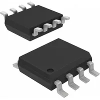
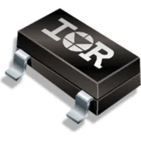
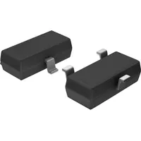
Onsemi MMBF170LT1G

|
|
||||
|
|
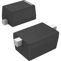
Unlock the power of next-generation technology with the MMBF170LT1G by Onsemi. As a leader in small signal field effect transistors, Onsemi delivers top-quality products that are perfect for switching applications. This N-CHANNEL transistor boasts a single configuration with a built-in diode, offering enhanced performance and reliability. With a maximum drain current of 0.5 A and a minimum DS breakdown voltage of 60V, this transistor is designed to handle high-power applications with ease. Trust Onsemi to provide you with the cutting-edge technology you need to take your projects to the next level.
Package Body Material: PLASTIC/EPOXY
Provides durability and protection for the transistor, making it suitable for various applications.
Polarity or Channel Type: N-CHANNEL
N-Channel FETs generally have better conductivity and lower on-resistance compared to P-Channel FETs, improving overall performance.
Transistor Application: SWITCHING
Designed specifically for switching applications, ensuring efficient and reliable performance in such scenarios.
Operating Mode: ENHANCEMENT MODE
Enhancement mode FETs offer better control and higher efficiency in operation, making them ideal for various electronic circuits.
Maximum Drain Current (Abs): 0.5 A
With a relatively high maximum drain current, this transistor can handle moderate power loads effectively.
Maximum Power Dissipation (Abs): 0.225 W
The low power dissipation helps in reducing heat generation and improving the overall efficiency of the device.
Maximum Operating Temperature: 150 °C
With a high maximum operating temperature, this transistor can withstand harsh environmental conditions and continue to function reliably.
Maximum Drain-Source On Resistance: 5 ohm
Low drain-source on resistance leads to minimal power loss and improved performance in high-frequency applications.
| Package Body Material: | PLASTIC/EPOXY |
| Maximum Time At Peak Reflow Temperature (s): | 40 |
| Configuration: | SINGLE WITH BUILT-IN DIODE |
| Transistor Element Material: | SILICON |
| Field Effect Transistor Technology: | METAL-OXIDE SEMICONDUCTOR |
| Transistor Application: | SWITCHING |
| Maximum Drain Current (ID): | .5 A |
| Sub-Category: | FET General Purpose Powers |
| Surface Mount: | YES |
| Terminal Finish: | Matte Tin (Sn) - annealed |
| No. of Terminals: | 3 |
| Maximum Power Dissipation (Abs): | .225 W |
| Terminal Position: | DUAL |
| Package Style (Meter): | SMALL OUTLINE |
| JESD-30 Code: | R-PDSO-G3 |
| No. of Elements: | 1 |
| Package Shape: | RECTANGULAR |
| Terminal Form: | GULL WING |
| Operating Mode: | ENHANCEMENT MODE |
| Maximum Operating Temperature: | 150 Cel |
| Maximum Drain-Source On Resistance: | 5 ohm |
| Moisture Sensitivity Level (MSL): | 1 |
| JEDEC-95 Code: | TO-236AB |
| Polarity or Channel Type: | N-CHANNEL |
| JESD-609 Code: | e3 |
| Minimum Operating Temperature: | -55 Cel |
| Minimum DS Breakdown Voltage: | 60 V |
| Qualification: | Not Qualified |
| Maximum Drain Current (Abs) (ID): | .5 A |
| Peak Reflow Temperature (C): | 260 |
| ECCN | EAR99 |
| ECCN Governance | EAR |
| HTS | 8541.29.00.95 |
| SB | 8541.29.00.80 |
