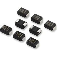
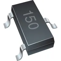
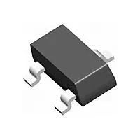
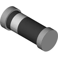
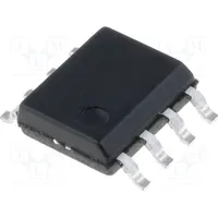
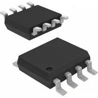
Diodes Incorporated BSS138DW-7-F

|
|
||||
|
|
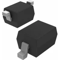
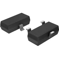
Experience the unmatched quality and innovation of Diodes Incorporated with the BSS138DW-7-F. This small signal field effect transistor offers exceptional performance and reliability, making it ideal for a wide range of applications. Its N-channel configuration and built-in diode provide seamless switching capabilities, while its compact rectangular package and gull wing terminals ensure easy surface mounting. With a minimum DS breakdown voltage of 50V and maximum drain current of 0.2A, this enhancement mode transistor delivers unparalleled power and efficiency. Trust Diodes Incorporated to deliver cutting-edge technology and superior value with the BSS138DW-7-F.
Package Body Material: PLASTIC/EPOXY
This material provides durability and protection for the small signal field effect transistor, making it a reliable choice for various applications.
Polarity or Channel Type: N-CHANNEL
The N-channel configuration enhances the performance of switching applications, providing efficient and reliable operation.
Configuration: SEPARATE, 2 ELEMENTS WITH BUILT-IN DIODE
The separate configuration with two elements and a built-in diode offers flexibility and versatility in circuit design, allowing for more efficient control and functionality.
Transistor Application: SWITCHING
Designed specifically for switching applications, this small signal field effect transistor can efficiently handle the switching of signals and provide accurate control.
Surface Mount: YES
With surface mount capability, this transistor can be easily attached to circuit boards, saving space and simplifying the overall design process.
Minimum DS Breakdown Voltage: 50 V
The minimum DS (Drain-Source) breakdown voltage of 50V ensures that the transistor can handle higher voltage levels, making it suitable for various voltage-dependent applications.
Package Shape: RECTANGULAR
The rectangular package shape allows for space-efficient circuit board layout, enabling easy integration of the transistor into the overall system design.
Terminal Form: GULL WING
The gull wing terminal form provides secure and reliable connections, ensuring proper electrical contact and reducing the risk of signal loss or faulty operation.
Operating Mode: ENHANCEMENT MODE
The enhancement mode operating mode enhances the transistor's performance in terms of speed and efficiency, making it an ideal choice for high-speed switching applications.
No. of Elements: 2
With two elements, this transistor offers increased functionality and versatility, allowing for the implementation of more complex circuit designs.
Maximum Drain Current (Abs) (ID): 0.2 A
With a maximum drain current of 0.2A, this transistor can handle higher current loads, making it suitable for applications that require reliable current control.
No. of Terminals: 6
The six terminals provide various connection options, enabling flexibility in circuit design and facilitating integration into the overall system.
Maximum Power Dissipation (Abs): 0.2 W
The maximum power dissipation of 0.2W ensures that the transistor can effectively dissipate heat generated during operation, enhancing its reliability and preventing overheating.
Package Style (Meter): SMALL OUTLINE
The small outline package style offers compactness and space-saving advantages, making it suitable for applications with limited board space.
Field Effect Transistor Technology: METAL-OXIDE SEMICONDUCTOR
The metal-oxide semiconductor technology used in this transistor ensures high performance, low power consumption, and improved overall efficiency.
Maximum Operating Temperature: 150 °C
With a maximum operating temperature of 150°C, this transistor can operate reliably even in demanding temperature conditions, enhancing its suitability for various environments.
Transistor Element Material: SILICON
The silicon element material provides excellent electrical properties, ensuring superior performance and reliability in small signal applications.
Terminal Finish: MATTE TIN
The matte tin terminal finish provides corrosion resistance and reliable electrical connections, increasing the lifespan and performance of the transistor.
Maximum Drain-Source On Resistance: 3.5 ohm
With a maximum drain-source on resistance of 3.5 ohms, this transistor offers low resistance, minimizing power loss and improving overall efficiency.
Terminal Position: DUAL
With a dual terminal position, this transistor offers flexible installation options, enabling different circuit configurations for enhanced versatility.
Maximum Time At Peak Reflow Temperature (s): 30
The maximum time at peak reflow temperature of 30 seconds ensures that the transistor can withstand the reflow soldering process without any damage, facilitating efficient manufacturing processes.
Peak Reflow Temperature °C: 260
With a peak reflow temperature of 260°C, this transistor can withstand high-temperature soldering processes, ensuring reliable and strong solder joints.
Maximum Feedback Capacitance (Crss): 8 pF
With a maximum feedback capacitance of 8 picofarads, this transistor exhibits low capacitance, minimizing signal loss and ensuring accurate signal control.
Reference Standard: AEC-Q101
Complying with the AEC-Q101 standard ensures that this transistor meets the stringent requirements of automotive applications, making it a reliable choice for automotive electronic systems.
| Package Body Material: | PLASTIC/EPOXY |
| Maximum Time At Peak Reflow Temperature (s): | 30 |
| Configuration: | SEPARATE, 2 ELEMENTS WITH BUILT-IN DIODE |
| Transistor Element Material: | SILICON |
| Field Effect Transistor Technology: | METAL-OXIDE SEMICONDUCTOR |
| Transistor Application: | SWITCHING |
| Maximum Drain Current (ID): | .2 A |
| Sub-Category: | FET General Purpose Power |
| Surface Mount: | YES |
| Terminal Finish: | MATTE TIN |
| No. of Terminals: | 6 |
| Maximum Power Dissipation (Abs): | .2 W |
| Terminal Position: | DUAL |
| Package Style (Meter): | SMALL OUTLINE |
| JESD-30 Code: | R-PDSO-G6 |
| No. of Elements: | 2 |
| Package Shape: | RECTANGULAR |
| Terminal Form: | GULL WING |
| Operating Mode: | ENHANCEMENT MODE |
| Maximum Operating Temperature: | 150 Cel |
| Maximum Drain-Source On Resistance: | 3.5 ohm |
| Moisture Sensitivity Level (MSL): | 1 |
| Other Names: | BSS138DW-FDICT<br>BSS138DW-FDIDKR<br>BSS138DW-FDITR<br>BSS138DW7F |
| Maximum Feedback Capacitance (Crss): | 8 pF |
| Polarity or Channel Type: | N-CHANNEL |
| JESD-609 Code: | e3 |
| Minimum DS Breakdown Voltage: | 50 V |
| Qualification: | Not Qualified |
| Additional Features: | HIGH RELIABILITY |
| Reference Standard: | AEC-Q101 |
| Maximum Drain Current (Abs) (ID): | .2 A |
| Peak Reflow Temperature (C): | 260 |
| ECCN | EAR99 |
| ECCN Governance | EAR |
