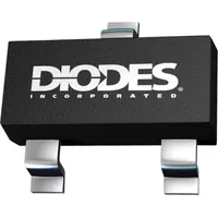
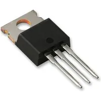
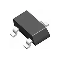
Onsemi FDV303N
|
|
||||
|
|
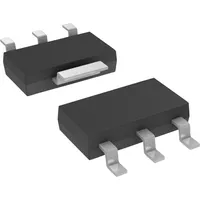
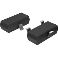
Enhance your electronic projects with the Onsemi FDV303N Small Signal Field Effect Transistor. Manufactured by a trusted name in the industry, Onsemi, this N-CHANNEL transistor offers reliable performance and quality you can count on. Ideal for switching applications, this transistor features a single configuration with a built-in diode, making it versatile and efficient for a variety of projects. With a maximum drain current of 0.68 A and a low on-resistance of 0.45 ohms, this transistor delivers high performance while saving space with its small outline package style. Experience the value and benefits of the FDV303N by Onsemi today!
Package Body Material: PLASTIC/EPOXY
Plastic/epoxy material provides durability and protection for the transistor, making it suitable for various applications.
Polarity or Channel Type: N-CHANNEL
N-channel transistors generally have better conductivity and efficiency compared to P-channel transistors, making this transistor suitable for high-performance applications.
Configuration: SINGLE WITH BUILT-IN DIODE
Built-in diode allows for better control and functionality in switching applications.
Transistor Application: SWITCHING
Designed specifically for switching applications, ensuring reliable performance in such scenarios.
Surface Mount: YES
Surface mount capability allows for easy and efficient PCB integration.
Minimum DS Breakdown Voltage: 25 V
With a minimum breakdown voltage of 25V, this transistor can handle higher voltages, making it suitable for a wide range of applications.
Package Shape: RECTANGULAR
Rectangular shape enhances the ease of PCB layout and assembly.
Terminal Form: GULL WING
Gull wing terminals provide secure connections and are ideal for surface mounting.
Operating Mode: ENHANCEMENT MODE
Enhancement mode operation allows for easy control of the transistor, leading to improved performance in switching applications.
Maximum Drain Current (Abs) (ID): 0.68 A
With a maximum drain current of 0.68A, this transistor can handle higher current loads, ensuring reliable operation.
No. of Terminals: 3
Three terminals provide standard connectivity for various circuit designs.
Maximum Power Dissipation (Abs): 0.35 W
With a maximum power dissipation of 0.35W, this transistor can handle moderate power levels efficiently.
Package Style (Meter): SMALL OUTLINE
Small outline package style saves space on the PCB, making it suitable for compact electronic devices.
Field Effect Transistor Technology: METAL-OXIDE SEMICONDUCTOR
Metal-oxide semiconductor technology ensures high reliability and performance in various operating conditions.
Maximum Operating Temperature: 150 °C
High maximum operating temperature of 150°C allows for reliable operation in elevated temperature environments.
Transistor Element Material: SILICON
Silicon-based transistor element offers excellent electronic properties and durability.
Minimum Operating Temperature: -55 °C
Low minimum operating temperature of -55°C ensures reliable performance in cold environments.
Terminal Finish: Matte Tin (Sn) - annealed
Matte tin finish provides corrosion resistance and ensures secure connections.
Maximum Drain Current (ID): 0.68 A
With a maximum drain current of 0.68A, this transistor can handle higher current loads efficiently.
Maximum Drain-Source On Resistance: 0.45 ohm
Low drain-source on resistance of 0.45 ohms ensures efficient performance in switching applications.
Terminal Position: DUAL
Dual terminal position provides flexibility in circuit connections.
Maximum Time At Peak Reflow Temperature (s): 30
With a maximum reflow time of 30s at peak temperature, the transistor can be soldered efficiently onto the PCB.
Peak Reflow Temperature °C: 260
High peak reflow temperature of 260°C ensures reliable soldering and connection integrity.
| Package Body Material: | PLASTIC/EPOXY |
| Maximum Time At Peak Reflow Temperature (s): | 30 |
| Configuration: | SINGLE WITH BUILT-IN DIODE |
| Transistor Element Material: | SILICON |
| Field Effect Transistor Technology: | METAL-OXIDE SEMICONDUCTOR |
| Transistor Application: | SWITCHING |
| Maximum Drain Current (ID): | .68 A |
| Sub-Category: | FET General Purpose Power |
| Surface Mount: | YES |
| Terminal Finish: | Matte Tin (Sn) - annealed |
| No. of Terminals: | 3 |
| Maximum Power Dissipation (Abs): | .35 W |
| Terminal Position: | DUAL |
| Package Style (Meter): | SMALL OUTLINE |
| JESD-30 Code: | R-PDSO-G3 |
| No. of Elements: | 1 |
| Package Shape: | RECTANGULAR |
| Terminal Form: | GULL WING |
| Operating Mode: | ENHANCEMENT MODE |
| Maximum Operating Temperature: | 150 Cel |
| Maximum Drain-Source On Resistance: | .45 ohm |
| Moisture Sensitivity Level (MSL): | 1 |
| Polarity or Channel Type: | N-CHANNEL |
| JESD-609 Code: | e3 |
| Minimum Operating Temperature: | -55 Cel |
| Minimum DS Breakdown Voltage: | 25 V |
| Qualification: | Not Qualified |
| Maximum Drain Current (Abs) (ID): | .68 A |
| Peak Reflow Temperature (C): | 260 |
| ECCN | EAR99 |
| ECCN Governance | EAR |

