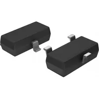
Diodes Incorporated BSS138K-13
|
|
||||
|
|
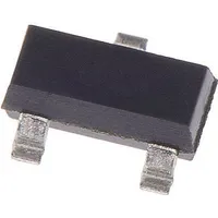
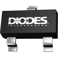
Elevate your circuit designs with the BSS138K-13 by Diodes Incorporated, a top-tier manufacturer known for delivering high-quality components. As part of the Small Signal Field Effect Transistors (FET) category, this N-CHANNEL transistor offers exceptional performance in switching applications. Its single configuration with built-in diode and enhancement mode operation make it a versatile choice for various projects. With a maximum power dissipation of 0.54W and a minimum DS breakdown voltage of 50V, this transistor ensures reliability and efficiency. Trust in Diodes Incorporated to provide you with the cutting-edge technology you need to take your designs to the next level.
Package Body Material: PLASTIC/EPOXY
This material offers good insulation properties and durability, ensuring reliable performance in various operating conditions.
Polarity or Channel Type: N-CHANNEL
N-channel FETs typically have higher mobility and conductivity, making them suitable for high-speed switching applications.
Configuration: SINGLE WITH BUILT-IN DIODE
The built-in diode provides additional protection against reverse voltage spikes, enhancing the reliability of the transistor.
Transistor Application: SWITCHING
Designed specifically for switching applications, this transistor offers fast switching speeds and low power consumption.
Surface Mount: YES
Surface mount packaging allows for easy integration into compact electronic devices, saving space on the PCB.
Minimum DS Breakdown Voltage: 50 V
With a high breakdown voltage, this transistor can handle higher voltages without breakdown, ensuring reliable operation in various circuit designs.
Package Shape: RECTANGULAR
Rectangular shape offers easy placement and alignment on the PCB, aiding in the manufacturing process.
Terminal Form: GULL WING
Gull wing terminals provide good mechanical strength and solderability, ensuring secure connections on the PCB.
Operating Mode: ENHANCEMENT MODE
Enhancement mode transistors are normally off and require a positive voltage to turn on, offering better control over the switching operation.
No. of Terminals: 3
Three terminals provide the necessary connections for the transistor to function effectively in the circuit.
Maximum Power Dissipation (Abs): 0.54 W
With a high power dissipation rating, this transistor can handle moderate power levels without overheating, increasing its reliability in operation.
Package Style (Meter): SMALL OUTLINE
Small outline packaging saves space on the PCB and allows for higher component density, ideal for compact electronic designs.
Field Effect Transistor Technology: METAL-OXIDE SEMICONDUCTOR
Metal-oxide semiconductor technology offers good performance and reliability in switching applications, making this transistor a reliable choice.
Maximum Operating Temperature: 150 °C
With a high operating temperature range, this transistor can withstand elevated temperatures without compromising performance, suitable for various environments.
Transistor Element Material: SILICON
Silicon-based transistors offer good electrical properties and reliability, ensuring stable performance in different operating conditions.
Minimum Operating Temperature: -55 °C
With a low minimum operating temperature, this transistor can function effectively in cold environments without performance degradation.
Terminal Finish: MATTE TIN
Matte tin finish provides good solderability and corrosion resistance, ensuring reliable connections on the PCB.
Maximum Drain Current (ID): 0.31 A
With a high drain current rating, this transistor can handle moderate current levels, suitable for various switching applications.
Maximum Drain-Source On Resistance: 3.5 ohm
Low drain-source on resistance ensures efficient power handling and minimal voltage drop across the transistor, improving overall circuit performance.
Terminal Position: DUAL
Dual terminal position allows for flexible mounting options and easy integration into different circuit designs.
Peak Reflow Temperature °C: 260
High peak reflow temperature ensures reliable solder joints during the assembly process, improving overall manufacturing quality.
Maximum Feedback Capacitance (Crss): 2.2 pF
Low feedback capacitance reduces signal distortion and improves high-frequency performance, making this transistor suitable for high-speed applications.
| Package Body Material: | PLASTIC/EPOXY |
| Configuration: | SINGLE WITH BUILT-IN DIODE |
| Transistor Element Material: | SILICON |
| Field Effect Transistor Technology: | METAL-OXIDE SEMICONDUCTOR |
| Transistor Application: | SWITCHING |
| Maximum Drain Current (ID): | .31 A |
| Surface Mount: | YES |
| Terminal Finish: | MATTE TIN |
| No. of Terminals: | 3 |
| Maximum Power Dissipation (Abs): | .54 W |
| Terminal Position: | DUAL |
| Package Style (Meter): | SMALL OUTLINE |
| JESD-30 Code: | R-PDSO-G3 |
| No. of Elements: | 1 |
| Package Shape: | RECTANGULAR |
| Terminal Form: | GULL WING |
| Operating Mode: | ENHANCEMENT MODE |
| Maximum Operating Temperature: | 150 Cel |
| Maximum Drain-Source On Resistance: | 3.5 ohm |
| Other Names: | BSS138K-13DICT<br>BSS138K-13DITR<br>BSS138K-13DIDKR |
| Maximum Feedback Capacitance (Crss): | 2.2 pF |
| Polarity or Channel Type: | N-CHANNEL |
| JESD-609 Code: | e3 |
| Minimum Operating Temperature: | -55 Cel |
| Minimum DS Breakdown Voltage: | 50 V |
| Peak Reflow Temperature (C): | 260 |
| ECCN | EAR99 |
| ECCN Governance | EAR |
