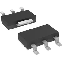
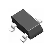
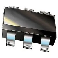
| Package Body Material: |
PLASTIC/EPOXY |
| Configuration: |
SINGLE WITH BUILT-IN DIODE |
| Transistor Element Material: |
SILICON |
| Field Effect Transistor Technology: |
METAL-OXIDE SEMICONDUCTOR |
| Transistor Application: |
SWITCHING |
| Maximum Turn On Time (ton): |
55 ns |
| Maximum Drain Current (ID): |
2.5 A |
| Maximum Pulsed Drain Current (IDM): |
15 A |
| Sub-Category: |
Other Transistors |
| Surface Mount: |
YES |
| Terminal Finish: |
Tin/Lead (Sn/Pb) |
| No. of Terminals: |
4 |
| Maximum Power Dissipation (Abs): |
3 W |
| Terminal Position: |
DUAL |
| Package Style (Meter): |
SMALL OUTLINE |
| Maximum Turn Off Time (toff): |
60 ns |
| JESD-30 Code: |
R-PDSO-G4 |
| No. of Elements: |
1 |
| Package Shape: |
RECTANGULAR |
| Terminal Form: |
GULL WING |
| Operating Mode: |
ENHANCEMENT MODE |
| Maximum Operating Temperature: |
150 Cel |
| Case Connection: |
DRAIN |
| Maximum Power Dissipation Ambient: |
1.1 W |
| Maximum Drain-Source On Resistance: |
.3 ohm |
| Other Names: |
NDT2955TR<br>NDT2955CT<br>NDT2955TR-NDR<br>NDT2955DKR<br>NDT2955CT-NDR<br>2832-NDT2955TR |
| JEDEC-95 Code: |
TO-261 |
| Polarity or Channel Type: |
P-CHANNEL |
| JESD-609 Code: |
e0 |
| Minimum DS Breakdown Voltage: |
60 V |
| Qualification: |
Not Qualified |
| Maximum Drain Current (Abs) (ID): |
2.5 A |
