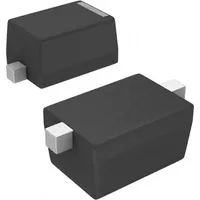
Onsemi BSS138LT1G

|
|
||||
|
|
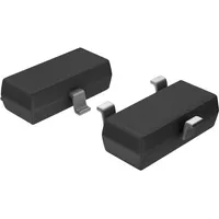
Enhance your electronic designs with the reliable BSS138LT1G by Onsemi. As a leading manufacturer in the industry, Onsemi delivers high-quality small signal field effect transistors that are perfect for switching applications. With a maximum drain current of 0.2 A and a minimum DS breakdown voltage of 50V, this N-channel transistor offers exceptional performance and efficiency. Its compact package body material and surface mount capability make it easy to integrate into your projects. Trust Onsemi to provide you with the tools you need to bring your ideas to life effortlessly.
Package Body Material: PLASTIC/EPOXY
Plastic/Epoxy material provides durability and protection for the transistor, making it suitable for a variety of applications.
Polarity or Channel Type: N-CHANNEL
N-Channel type offers better performance in terms of power efficiency and speed compared to P-Channel transistors.
Configuration: SINGLE WITH BUILT-IN DIODE
Built-in diode allows for protection against reverse current flow and simplifies circuit design.
Transistor Application: SWITCHING
Designed specifically for switching applications, ensuring reliable performance in ON/OFF states.
Surface Mount: YES
Surface mount capability enables easy and efficient assembly onto circuit boards.
Minimum DS Breakdown Voltage: 50 V
Sufficient breakdown voltage ensures reliable operation under varying load conditions.
Maximum Drain Current (ID): 0.2 A
Can handle a maximum drain current of 0.2 A, suitable for low power applications.
Maximum Power Dissipation: 0.225 W
With a maximum power dissipation of 0.225 W, it can operate efficiently without overheating.
Maximum Operating Temperature: 150 °C
Wide operating temperature range of -55 to 150 °C ensures reliable performance in various environments.
Field Effect Transistor Technology: METAL-OXIDE SEMICONDUCTOR
Metal-Oxide Semiconductor technology offers low power consumption and high efficiency.
| Package Body Material: | PLASTIC/EPOXY |
| Maximum Time At Peak Reflow Temperature (s): | 40 |
| Configuration: | SINGLE WITH BUILT-IN DIODE |
| Transistor Element Material: | SILICON |
| Field Effect Transistor Technology: | METAL-OXIDE SEMICONDUCTOR |
| Transistor Application: | SWITCHING |
| Maximum Drain Current (ID): | .2 A |
| Sub-Category: | FET General Purpose Powers |
| Surface Mount: | YES |
| Terminal Finish: | Matte Tin (Sn) - annealed |
| No. of Terminals: | 3 |
| Maximum Power Dissipation (Abs): | .225 W |
| Terminal Position: | DUAL |
| Package Style (Meter): | SMALL OUTLINE |
| JESD-30 Code: | R-PDSO-G3 |
| No. of Elements: | 1 |
| Package Shape: | RECTANGULAR |
| Terminal Form: | GULL WING |
| Operating Mode: | ENHANCEMENT MODE |
| Maximum Operating Temperature: | 150 Cel |
| Maximum Drain-Source On Resistance: | 3.5 ohm |
| Moisture Sensitivity Level (MSL): | 1 |
| Other Names: | 2156-BSS138LT1G-OS<br>BSS138LT1GOSTR<br>BSS138LT1GOSCT<br>BSS138LT1GOSDKR<br>2832-BSS138LT1G-488<br>ONSONSBSS138LT1G |
| Maximum Feedback Capacitance (Crss): | 5 pF |
| JEDEC-95 Code: | TO-236 |
| Polarity or Channel Type: | N-CHANNEL |
| JESD-609 Code: | e3 |
| Minimum Operating Temperature: | -55 Cel |
| Minimum DS Breakdown Voltage: | 50 V |
| Qualification: | Not Qualified |
| Maximum Drain Current (Abs) (ID): | .2 A |
| Peak Reflow Temperature (C): | 260 |
| ECCN | EAR99 |
| ECCN Governance | EAR |
| NSN | 5961-01-633-5321, 5961016335321 |
| NIIN | 016335321 |

