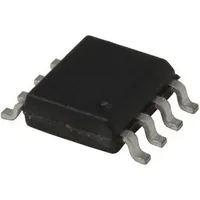
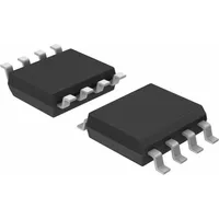
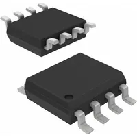
Texas Instruments LM358MX
|
|
||||
|
|
Experience high-quality performance and versatility with the LM358MX by Texas Instruments. As a leading manufacturer in operational amplifiers (Op Amps), Texas Instruments ensures exceptional reliability and precision in every product. The LM358MX offers a wide range of applications, making it ideal for various industries. With its compact design and surface mount capability, this amplifier delivers convenience and flexibility. Its impressive features include a maximum input offset voltage of 9000 uV and a nominal common mode reject ratio of 85 dB, guaranteeing accurate and efficient operation. Whether you need reliable amplification for audio systems or precise signal conditioning in industrial automation, the LM358MX provides excellent value, benefits, and advantages to meet your specific needs. Trust Texas Instruments for superior quality and performance.
Package Body Material: PLASTIC/EPOXY
The plastic/epoxy package provides durability and resistance to environmental factors, making it suitable for a wide range of applications.
Maximum Input Offset Voltage: 9000 uV
A low input offset voltage ensures accurate signal amplification, making it ideal for precision applications.
Maximum Average Bias Current (IIB): 0.05 uA
This low bias current ensures minimal input errors, improving overall performance in high-impedance circuits.
Surface Mount: YES
Surface mount technology allows for easy integration into modern compact designs, enhancing design flexibility.
No. of Functions: 2
Having multiple functions increases versatility for different circuit designs, providing more value.
Package Shape: RECTANGULAR
The rectangular package shape allows for efficient use of board space in circuit designs.
Nominal Common Mode Reject Ratio: 85 dB
A high common-mode rejection ratio enhances signal integrity by reducing noise interference, making it suitable for sensitive applications.
Nominal Supply Voltage / Vsup (V): 5
This nominal supply voltage aligns well with common logic levels, simplifying design considerations.
Power Supplies (V): ±1.5/±15/3/30
Flexible power supply options make this op-amp adaptable to various system requirements.
No. of Terminals: 8
An 8-terminal configuration provides sufficient connectivity for complex circuits while maintaining a compact size.
Maximum Input Offset Current (IIO): 0.05 uA
Low input offset current contributes to improved accuracy in signal processing applications.
Package Style (Meter): SMALL OUTLINE
The small outline package style enables space-saving designs, which are crucial for modern electronic devices.
Maximum Supply Voltage Limit: 32 V
A high supply voltage limit allows the op-amp to operate in various applications with different voltage requirements.
Maximum Operating Temperature: 70 °C
This temperature capability ensures stable operation in a variety of environments and applications.
Maximum Bias Current (IIB) @25°C: 0.15 uA
The low bias current at typical operating temperatures maintains accuracy in high-impedance scenarios.
Frequency Compensation: YES
Built-in frequency compensation enhances circuit stability, especially in feedback arrangements.
Minimum Voltage Gain: 15000
A high voltage gain ensures significant amplification of weak signals, making it a strong choice for signal processing.
Minimum Operating Temperature: 0 °C
The minimum operating temperature allows for use in various environmental conditions, enhancing application range.
Terminal Finish: TIN LEAD
Tin-lead finish provides good solderability and reliability in connections, ensuring longevity in use.
Terminal Position: DUAL
Dual terminal positions are beneficial for ease of layout in PCB designs, allowing for better routing.
Maximum Seated Height: 1.75 mm
A compact height facilitates integration into slim form factor applications.
Width: 3.9 mm
The narrow width of the package is advantageous for tightly packed circuit designs.
Maximum Time At Peak Reflow Temperature: 20 s
A manageable reflow time supports mass production without damaging the component.
Peak Reflow Temperature: 235 °C
This temperature rating ensures compatibility with standard soldering processes in manufacturing.
Length: 4.9 mm
A compact length aids in saving PCB space, allowing for denser circuit designs.
Temperature Grade: COMMERCIAL
Commercial temperature grade makes this component suitable for a wide range of consumer electronics.
Maximum Negative Supply Voltage Limit: 0 V
The limited negative supply voltage makes the op-amp suitable for single-supply applications.
Nominal Unity Gain Bandwidth: 1000 kHz
A high unity gain bandwidth ensures effective performance in a variety of high-frequency applications.
Minimum Common Mode Reject Ratio: 65 dB
While lower than the nominal, this still provides decent noise suppression, enhancing overall signal quality.
Technology: BIPOLAR
Bipolar technology typically offers faster response times and better performance for certain applications.
Terminal Form: GULL WING
Gull-wing terminals facilitate easier handling and soldering in PCB assembly.
Amplifier Type: OPERATIONAL AMPLIFIER
Being an operational amplifier, it is fundamentally designed for analog signal processing tasks, adding versatility.
Maximum Supply Current: 1.2 mA
Low supply current consumption contributes to power efficiency in battery-operated and portable devices.
Nominal Negative Supply Voltage (Vsup): 0 V
This design aligns with many modern single-supply systems, simplifying circuit configurations.
Architecture: VOLTAGE-FEEDBACK
Voltage-feedback architecture provides flexibility in design and a wide range of applications.
Packing Method: TR
Tape and reel packing method enables efficient handling and automated placement during manufacturing.
Nominal Slow Rate: 0.1 V/us
A nominal slow rate allows for controlled signal transitions, reducing the potential for signal distortion.
Terminal Pitch: 1.27 mm
A standard terminal pitch makes it compatible with various PCB designs and reduces assembly complexity.
| Package Body Material: | Plastic/Epoxy |
| Maximum Time At Peak Reflow Temperature (s): | 20 s |
| Low-Bias: | No |
| Sub-Category: | Operational Amplifiers |
| Surface Mount: | Yes |
| Maximum Input Offset Voltage: | 9000 uV |
| Technology: | BIPOLAR |
| Minimum Voltage Gain: | 15000 |
| Package Shape: | Rectangular |
| Terminal Form: | Gull Wing |
| Package Code: | SOP |
| Amplifier Type: | Operational Amplifier |
| Nominal Slow Rate: | 0.1 V/us |
| Moisture Sensitivity Level (MSL): | 1 |
| Architecture: | Voltage Feedback |
| Packing Method: | Tape And Reel |
| Programmable Power: | No |
| Nominal Negative Supply Voltage (Vsup): | 0 V |
| Qualification: | No |
| Package Equivalence Code: | SOP8,.25 |
| Peak Reflow Temperature (C): | 235 °C (455 °F) |
| Terminal Pitch: | 0.05 in (1.27 mm) |
| Maximum Seated Height: | 0.069 in (1.75 mm) |
| Frequency Compensation: | Yes |
| Maximum Supply Voltage Limit: | 32 V |
| Maximum Bias Current (IIB) @25C: | 150 nA |
| Maximum Supply Current: | 1.2 mA |
| Terminal Finish: | Tin Lead |
| No. of Terminals: | 8 |
| Nominal Unity Gain Bandwidth: | 1 MHz |
| Terminal Position: | Dual |
| Package Style (Meter): | Small Outline |
| JESD-30 Code: | R-PDSO-G8 |
| Low-Offset: | No |
| Maximum Operating Temperature: | 70 °C (158 °F) |
| Width: | 0.154 in (3.9 mm) |
| Nominal Common Mode Reject Ratio: | 85 dB |
| Micropower: | No |
| JESD-609 Code: | e0 |
| Minimum Operating Temperature: | 0 °C (32 °F) |
| Maximum Average Bias Current (IIB): | 50 nA |
| No. of Functions: | 2 |
| Minimum Common Mode Reject Ratio: | 65 dB |
| Length: | 0.193 in (4.9 mm) |
| Nominal Supply Voltage / Vsup (V): | 5 V |
| Maximum Negative Supply Voltage Limit: | 0 V |
| Maximum Input Offset Current (IIO): | 50 nA |
| Power: | No |
| Temperature Grade: | Commercial |
| Wideband: | No |
| Power Supplies (V): | ±1.5/±15/3/30 V |
| ECCN | EAR99 |
| ECCN Governance | EAR |
| HTS | 8542.33.00.01 |
| SB | 8542.33.00.00 |
