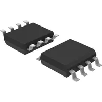
Vishay Intertechnology 2N7002-T1-E3

|
|
||||
|
|
Unleash the power of cutting-edge technology with the 2N7002-T1-E3 by Vishay Intertechnology. Crafted with precision and expertise, this Small Signal Field Effect Transistor offers unparalleled performance in switching applications. With a sleek design and high-quality construction, this N-Channel transistor is a game-changer in the world of electronics. Experience seamless operation and enhanced efficiency with the 2N7002-T1-E3. Elevate your projects to new heights with this innovative solution from Vishay Intertechnology.
Package Body Material: PLASTIC/EPOXY
Provides durability and protection for the transistor, making it suitable for various applications.
Polarity or Channel Type: N-CHANNEL
N-Channel transistors typically have better performance characteristics and are commonly used in switching applications.
Configuration: SINGLE
Simplified design with a single transistor for easier installation and maintenance.
Transistor Application: SWITCHING
Designed specifically for switching applications, ensuring efficient performance in those scenarios.
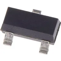
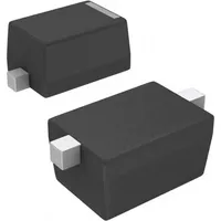
Surface Mount: YES
Easily mounted on PCBs, facilitating automated assembly processes and saving space.
Minimum DS Breakdown Voltage: 60 V
Can handle relatively high voltages, expanding the range of applications where it can be used.
Maximum Drain Current (Abs) (ID): 0.115 A
Can handle moderate current loads, suitable for many small signal applications.
Maximum Power Dissipation (Abs): 0.2 W
Efficient power handling capability for its size, ensuring reliable operation.
Field Effect Transistor Technology: METAL-OXIDE SEMICONDUCTOR
Known for low power consumption and high switching speeds, enhancing overall performance.
Maximum Operating Temperature: 150 °C
Can operate in higher temperature environments, expanding its range of applications.
Maximum Drain-Source On Resistance: 7.5 ohm
Low on-resistance minimizes power loss and heat generation, improving efficiency.
| Package Body Material: | PLASTIC/EPOXY |
| Maximum Time At Peak Reflow Temperature (s): | 30 |
| Configuration: | SINGLE |
| Transistor Element Material: | SILICON |
| Field Effect Transistor Technology: | METAL-OXIDE SEMICONDUCTOR |
| Transistor Application: | SWITCHING |
| Maximum Drain Current (ID): | .115 A |
| Sub-Category: | FET General Purpose Powers |
| Surface Mount: | YES |
| Terminal Finish: | MATTE TIN |
| No. of Terminals: | 3 |
| Maximum Power Dissipation (Abs): | .2 W |
| Terminal Position: | DUAL |
| Package Style (Meter): | SMALL OUTLINE |
| JESD-30 Code: | R-PDSO-G3 |
| No. of Elements: | 1 |
| Package Shape: | RECTANGULAR |
| Terminal Form: | GULL WING |
| Operating Mode: | ENHANCEMENT MODE |
| Maximum Operating Temperature: | 150 Cel |
| Maximum Drain-Source On Resistance: | 7.5 ohm |
| Moisture Sensitivity Level (MSL): | 1 |
| Other Names: | 2N7002-T1-E3TR<br>2N7002-T1-E3DKR<br>2N7002-T1-E3-ND<br>2N7002-T1-E3CT |
| Maximum Feedback Capacitance (Crss): | 5 pF |
| JEDEC-95 Code: | TO-236 |
| Polarity or Channel Type: | N-CHANNEL |
| JESD-609 Code: | e3 |
| Minimum Operating Temperature: | -55 Cel |
| Minimum DS Breakdown Voltage: | 60 V |
| Qualification: | Not Qualified |
| Additional Features: | LOW THRESHOLD |
| Maximum Drain Current (Abs) (ID): | .115 A |
| Peak Reflow Temperature (C): | 260 |
| ECCN | EAR99 |
| ECCN Governance | EAR |

