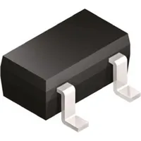
Onsemi FDC5614P
|
|
||||
|
|
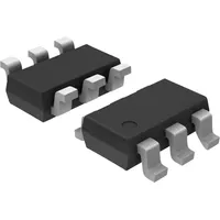
Enhance your power management capabilities with the FDC5614P by Onsemi. Designed with precision and reliability in mind, this P-channel Power FET offers seamless switching for a variety of applications. From enhancing efficiency to improving performance, this transistor is a game-changer in the field. Trust in Onsemi's reputation for quality and innovation, and unlock the full potential of your power systems with the FDC5614P. Elevate your projects and experience unparalleled value with this cutting-edge component.
Package Body Material: PLASTIC/EPOXY
Provides durability and protection for the power field effect transistor, making it suitable for various applications.
Polarity or Channel Type: P-CHANNEL
P-channel FETs are known for their low resistance and high current-carrying capabilities.
Transistor Application: SWITCHING
Designed for efficient switching applications, ensuring fast and reliable operation.
Minimum DS Breakdown Voltage: 60 V
With a high breakdown voltage, this FET can handle higher voltages without breakdown, ensuring durability.
Maximum Drain Current (Abs) (ID): 3 A
Capable of handling high currents, making it suitable for power applications.
Maximum Power Dissipation (Abs): 1.6 W
Efficient power dissipation capability, ensuring stable performance under high load conditions.
Maximum Operating Temperature: 150 °C
Can operate at high temperatures, suitable for industrial and automotive applications where heat may be a concern.
Maximum Turn On Time (ton): 34 ns
Fast turn-on time ensures quick response in switching applications, improving overall efficiency.
Maximum Turn Off Time (toff): 56 ns
Fast turn-off time reduces the chances of power loss and overheating, making it a reliable choice for switching applications.
| Package Body Material: | PLASTIC/EPOXY |
| Maximum Time At Peak Reflow Temperature (s): | 30 |
| Configuration: | SINGLE WITH BUILT-IN DIODE |
| Transistor Element Material: | SILICON |
| Field Effect Transistor Technology: | METAL-OXIDE SEMICONDUCTOR |
| Transistor Application: | SWITCHING |
| Maximum Turn On Time (ton): | 34 ns |
| Maximum Drain Current (ID): | 3 A |
| Maximum Pulsed Drain Current (IDM): | 20 A |
| Sub-Category: | Other Transistors |
| Surface Mount: | YES |
| Terminal Finish: | MATTE TIN |
| No. of Terminals: | 6 |
| Maximum Power Dissipation (Abs): | 1.6 W |
| Terminal Position: | DUAL |
| Package Style (Meter): | SMALL OUTLINE |
| Maximum Turn Off Time (toff): | 56 ns |
| JESD-30 Code: | R-PDSO-G6 |
| No. of Elements: | 1 |
| Package Shape: | RECTANGULAR |
| Terminal Form: | GULL WING |
| Operating Mode: | ENHANCEMENT MODE |
| Maximum Operating Temperature: | 150 Cel |
| Maximum Drain-Source On Resistance: | .105 ohm |
| Moisture Sensitivity Level (MSL): | 1 |
| Maximum Feedback Capacitance (Crss): | 39 pF |
| Polarity or Channel Type: | P-CHANNEL |
| JESD-609 Code: | e3 |
| Minimum Operating Temperature: | -55 Cel |
| Minimum DS Breakdown Voltage: | 60 V |
| Qualification: | Not Qualified |
| Maximum Drain Current (Abs) (ID): | 3 A |
| Peak Reflow Temperature (C): | 260 |
| ECCN | EAR99 |
| ECCN Governance | EAR |
