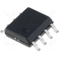
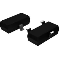
Onsemi FDN5618P
|
|
||||
|
|
Enhance your electronic devices with the high-quality FDN5618P Power Field Effect Transistor by Onsemi. Designed for switching applications, this P-CHANNEL transistor offers a single configuration with a built-in diode, providing convenience and efficiency. With a maximum drain current of 1.25 A and a minimum DS breakdown voltage of 60 V, this transistor ensures reliable performance. Whether you're working on power management or motor control systems, the FDN5618P delivers exceptional value and benefits, making it a top choice for electronics enthusiasts and professionals alike.
Package Body Material: PLASTIC/EPOXY
The plastic/epoxy material used for the package body provides good insulation and protection for the internal components of the FET.
Polarity or Channel Type: P-CHANNEL
P-channel FETs are known for their low ON resistance and high current-carrying capability, making them ideal for high-power switching applications.
Configuration: SINGLE WITH BUILT-IN DIODE
The built-in diode simplifies circuit design and protects against reverse voltage spikes, enhancing the reliability of the FET.
Transistor Application: SWITCHING
Designed specifically for switching applications, this FET offers fast switching speeds and low ON-resistance for efficient power control.
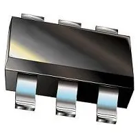
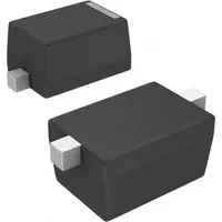
Surface Mount: YES
Surface mount technology allows for easy and efficient assembly onto PCBs, saving space and reducing manufacturing costs.
Minimum DS Breakdown Voltage: 60 V
With a high breakdown voltage, this FET can safely handle higher voltages, providing added protection for the circuit.
Maximum Drain Current (ID): 1.25 A
The high maximum drain current rating allows for superior power-handling capabilities, making it suitable for a variety of high-current applications.
Maximum Power Dissipation (Abs): 0.5 W
The low power dissipation helps in reducing heat generation and improving efficiency, leading to better overall performance of the FET.
Maximum Operating Temperature: 150 °C
With a high maximum operating temperature, this FET can withstand elevated temperatures without compromising its performance, ensuring reliability in harsh environments.
| Package Body Material: | PLASTIC/EPOXY |
| Maximum Time At Peak Reflow Temperature (s): | 30 |
| Configuration: | SINGLE WITH BUILT-IN DIODE |
| Transistor Element Material: | SILICON |
| Field Effect Transistor Technology: | METAL-OXIDE SEMICONDUCTOR |
| Transistor Application: | SWITCHING |
| Maximum Drain Current (ID): | 1.25 A |
| Maximum Pulsed Drain Current (IDM): | 10 A |
| Sub-Category: | Other Transistors |
| Surface Mount: | YES |
| Terminal Finish: | MATTE TIN |
| No. of Terminals: | 3 |
| Maximum Power Dissipation (Abs): | .5 W |
| Terminal Position: | DUAL |
| Package Style (Meter): | SMALL OUTLINE |
| JESD-30 Code: | R-PDSO-G3 |
| No. of Elements: | 1 |
| Package Shape: | RECTANGULAR |
| Terminal Form: | GULL WING |
| Operating Mode: | ENHANCEMENT MODE |
| Maximum Operating Temperature: | 150 Cel |
| Maximum Drain-Source On Resistance: | .17 ohm |
| Moisture Sensitivity Level (MSL): | 1 |
| Polarity or Channel Type: | P-CHANNEL |
| JESD-609 Code: | e3 |
| Minimum Operating Temperature: | -55 Cel |
| Minimum DS Breakdown Voltage: | 60 V |
| Qualification: | Not Qualified |
| Maximum Drain Current (Abs) (ID): | 1.25 A |
| Peak Reflow Temperature (C): | 260 |
| ECCN | EAR99 |
| ECCN Governance | EAR |

