Vishay Intertechnology 2N7002

|
|
||||
|
|
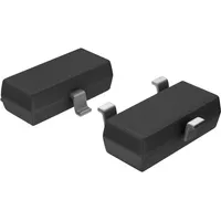
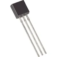
Looking for a reliable small signal field effect transistor for your switching applications? Look no further than the Vishay Intertechnology 2N7002. With its high-quality construction and N-CHANNEL polarity, this transistor offers superior performance and durability. Whether you need to switch circuits or control power flow, this transistor is the perfect solution. Trust Vishay Intertechnology for all your semiconductor needs and experience the value and benefits of their top-notch products.
Package Body Material: PLASTIC/EPOXY
Provides durability and protection for the transistor, making it suitable for a range of applications.
Polarity or Channel Type: N-CHANNEL
Offers good conductivity and performance in N-channel applications.
Configuration: SINGLE WITH BUILT-IN DIODE
Convenient built-in diode allows for versatile functionality in switching applications.
Transistor Application: SWITCHING
Specifically designed for switching applications, ensuring reliable performance in such scenarios.
Surface Mount: YES
Easy to mount on PCBs, saving space and making the product suitable for compact designs.
Minimum DS Breakdown Voltage: 60 V
With a high breakdown voltage, this transistor can handle higher voltages, improving its versatility.
Maximum Power Dissipation (Abs): 0.2 W
Efficient power usage and heat dissipation, ensuring reliable performance under varying conditions.
Maximum Operating Temperature: 150 °C
Can operate reliably at high temperatures, making it suitable for various industrial applications.
Transistor Element Material: SILICON
Common semiconductor material known for its reliability and performance in electronic devices.
Maximum Drain-Source On Resistance: 7.5 ohm
Low on-resistance leads to efficient power usage and minimal heat generation in the transistor.
| Package Body Material: | PLASTIC/EPOXY |
| Configuration: | SINGLE WITH BUILT-IN DIODE |
| Transistor Element Material: | SILICON |
| Field Effect Transistor Technology: | METAL-OXIDE SEMICONDUCTOR |
| Transistor Application: | SWITCHING |
| Maximum Drain Current (ID): | .115 A |
| Sub-Category: | FET General Purpose Power |
| Surface Mount: | YES |
| Terminal Finish: | Tin/Lead (Sn/Pb) |
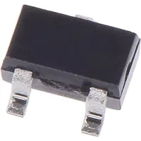
| No. of Terminals: | 3 |
| Maximum Power Dissipation (Abs): | .2 W |
| Terminal Position: | DUAL |
| Package Style (Meter): | SMALL OUTLINE |
| JESD-30 Code: | R-PDSO-G3 |
| No. of Elements: | 1 |
| Package Shape: | RECTANGULAR |
| Terminal Form: | GULL WING |
| Operating Mode: | ENHANCEMENT MODE |
| Maximum Operating Temperature: | 150 Cel |
| Maximum Power Dissipation Ambient: | .2 W |
| Maximum Drain-Source On Resistance: | 7.5 ohm |
| Maximum Feedback Capacitance (Crss): | 5 pF |
| JEDEC-95 Code: | TO-236 |
| Polarity or Channel Type: | N-CHANNEL |
| JESD-609 Code: | e0 |
| Minimum Operating Temperature: | -55 Cel |
| Minimum DS Breakdown Voltage: | 60 V |
| Maximum Drain Current (Abs) (ID): | .115 A |
| ECCN | EAR99 |
| ECCN Governance | EAR |
| HTS | 8541.21.00.95 |
| SB | 8541.21.00.80 |
| NSN | 5961-01-364-7859, 5961013647859, 5961-01-615-7494, 5961016157494 |
| NIIN | 013647859, 016157494 |
