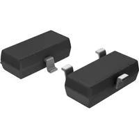
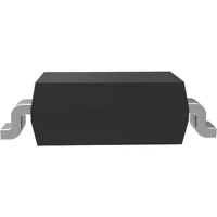
Micro Commercial Components BSS138-TP
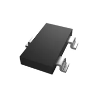
|
|
||||
|
|
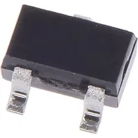
Discover the BSS138-TP by Micro Commercial Components, a top-of-the-line Small Signal Field Effect Transistor that guarantees high-quality and reliability. With its N-CHANNEL configuration and SINGLE WITH BUILT-IN DIODE design, this advanced transistor is perfect for a wide range of applications. Whether you're working on electronics, telecommunications, or automotive projects, the BSS138-TP is the ideal choice. Experience enhanced performance and efficiency with its low Drain-Source On Resistance and maximum Drain Current of 0.22 A. Trust in Micro Commercial Components' expertise and unlock the full potential of your projects.
Package Body Material: PLASTIC/EPOXY
This material provides durability and protection, making the product resistant to damage and suitable for various environments.
Polarity or Channel Type: N-CHANNEL
The N-channel type allows for efficient and controlled electron flow, enabling high-performance and reliable operation.
Configuration: SINGLE WITH BUILT-IN DIODE
The built-in diode offers reverse polarity protection and simplifies circuit design, enhancing the overall functionality and efficiency of the product.
Surface Mount: YES
The surface mount capability enables easy and precise placement on circuit boards, ensuring seamless integration and simplifying the manufacturing process.
Minimum DS Breakdown Voltage: 50 V
With a high breakdown voltage, this product can handle higher voltages without compromising its performance, providing added safety and reliability.
Package Shape: RECTANGULAR
The rectangular package shape allows for compact and space-efficient designs, making it ideal for applications with limited space.
Terminal Form: GULL WING
The gull wing terminal form facilitates easy soldering and provides secure connection points, ensuring optimal electrical contact for consistent performance.
Operating Mode: ENHANCEMENT MODE
The enhancement mode operation offers improved control over the transistor's behavior and enables efficient use in a wide range of applications.
No. of Elements: 1
With a single element, this product is compact and cost-effective, making it suitable for various small signal applications.
No. of Terminals: 3
Having three terminals allows for precise control and flexibility in circuit design, accommodating a wide range of applications.
Package Style (Meter): SMALL OUTLINE
The small outline package style provides easy integration into space-constrained designs, allowing for efficient and compact circuit layouts.
Field Effect Transistor Technology: METAL-OXIDE SEMICONDUCTOR
This technology ensures high-speed switching, low power consumption, and low distortion, making it an excellent choice for amplification and signal processing applications.
Transistor Element Material: SILICON
Silicon offers excellent thermal stability, high voltage capability, and low leakage current, resulting in reliable and long-lasting performance.
Terminal Finish: MATTE TIN
The matte tin terminal finish enhances solderability and provides corrosion resistance, ensuring robust and reliable connections.
Maximum Drain Current (ID): 0.22 A
With a high maximum drain current capability, this product can handle demanding applications, allowing for efficient power handling and high performance.
Maximum Drain-Source On Resistance: 3 ohm
The low drain-source on resistance minimizes power loss and enhances efficiency, making this product suitable for demanding applications.
Terminal Position: DUAL
Dual terminal position allows for versatile mounting and facilitates easy PCB layout, offering flexibility in design and installation.
Moisture Sensitivity Level (MSL): 1
The moisture sensitivity level 1 ensures that the product is well-protected during shipping and storage, maintaining its quality and reliability.
Maximum Time At Peak Reflow Temperature (s): 10
This product can withstand peak reflow temperatures for up to 10 seconds, making it suitable for high-temperature assembly processes without compromising its performance.
Peak Reflow Temperature °C: 260
With a high peak reflow temperature tolerance, this product can endure high-temperature soldering processes, offering reliable and robust solder joints.
| Other Names: | BSS138-TPMSDKR<br>BSS138-TPMSTR<br>BSS138-TPMSCT |
| Package Body Material: | PLASTIC/EPOXY |
| Maximum Time At Peak Reflow Temperature (s): | 10 |
| Configuration: | SINGLE WITH BUILT-IN DIODE |
| Transistor Element Material: | SILICON |
| Field Effect Transistor Technology: | METAL-OXIDE SEMICONDUCTOR |
| Maximum Drain Current (ID): | .22 A |
| Polarity or Channel Type: | N-CHANNEL |
| Surface Mount: | YES |
| Terminal Finish: | MATTE TIN |
| JESD-609 Code: | e3 |
| No. of Terminals: | 3 |
| Minimum DS Breakdown Voltage: | 50 V |
| Terminal Position: | DUAL |
| Package Style (Meter): | SMALL OUTLINE |
| JESD-30 Code: | R-PDSO-G3 |
| No. of Elements: | 1 |
| Package Shape: | RECTANGULAR |
| Terminal Form: | GULL WING |
| Operating Mode: | ENHANCEMENT MODE |
| Peak Reflow Temperature (C): | 260 |
| Maximum Drain-Source On Resistance: | 3 ohm |
| Moisture Sensitivity Level (MSL): | 1 |
| ECCN | EAR99 |
| ECCN Governance | EAR |


