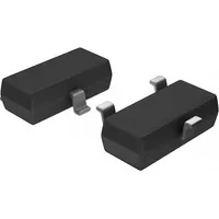
Onsemi BSS123LT1G
|
|
||||
|
|
Discover the BSS123LT1G by Onsemi, a top-quality small signal field effect transistor that offers unparalleled performance and reliability. Manufactured by Onsemi, a trusted name in the industry, this N-channel transistor is ideal for switching applications. With its single configuration and built-in diode, this transistor provides seamless operation and efficient power management. Whether you're looking to enhance your electronics projects or streamline your circuit design, the BSS123LT1G delivers the value, benefits, and advantages that customers seek. Experience innovation at its best with the BSS123LT1G.
Package Body Material: PLASTIC/EPOXY
Provides durability and protection for the transistor, ensuring a longer lifespan.
Polarity or Channel Type: N-CHANNEL
Allows for efficient electron flow and high conductivity in the transistor.
Configuration: SINGLE WITH BUILT-IN DIODE
Simplifies circuit design by incorporating a diode within the transistor itself.
Transistor Application: SWITCHING
Ideal for switching applications due to its fast response time and low power dissipation.
Surface Mount: YES
Enables easy and efficient mounting onto circuit boards.
Minimum DS Breakdown Voltage: 100 V
Ensures reliable operation under high voltage conditions.
Maximum Drain Current (Abs) (ID): 0.17 A
Handles high current levels effectively, suitable for various applications.
Maximum Power Dissipation (Abs): 0.225 W
Efficiently dissipates heat to prevent overheating and ensure stability.
Maximum Operating Temperature: 150 °C
Can withstand high operating temperatures, suitable for demanding environments.
Maximum Drain-Source On Resistance: 6 ohm
Provides low resistance for efficient current flow and minimal power loss.
| Package Body Material: | PLASTIC/EPOXY |
| Maximum Time At Peak Reflow Temperature (s): | 40 |
| Configuration: | SINGLE WITH BUILT-IN DIODE |
| Transistor Element Material: | SILICON |
| Field Effect Transistor Technology: | METAL-OXIDE SEMICONDUCTOR |
| Transistor Application: | SWITCHING |
| Maximum Drain Current (ID): | .17 A |
| Sub-Category: | FET General Purpose Power |
| Surface Mount: | YES |
| Terminal Finish: | Matte Tin (Sn) - annealed |
| No. of Terminals: | 3 |
| Maximum Power Dissipation (Abs): | .225 W |
| Terminal Position: | DUAL |
| Package Style (Meter): | SMALL OUTLINE |
| JESD-30 Code: | R-PDSO-G3 |
| No. of Elements: | 1 |
| Package Shape: | RECTANGULAR |
| Terminal Form: | GULL WING |
| Operating Mode: | ENHANCEMENT MODE |
| Maximum Operating Temperature: | 150 Cel |
| Maximum Drain-Source On Resistance: | 6 ohm |
| Moisture Sensitivity Level (MSL): | 1 |
| Other Names: | BSS123LT1GOSCT<br>BSS123LT1GOSTR<br>BSS123LT1GOSDKR<br>2156-BSS123LT1G-OS<br>ONSONSBSS123LT1G |
| JEDEC-95 Code: | TO-236 |
| Polarity or Channel Type: | N-CHANNEL |
| JESD-609 Code: | e3 |
| Minimum Operating Temperature: | -55 Cel |
| Minimum DS Breakdown Voltage: | 100 V |
| Qualification: | Not Qualified |
| Maximum Drain Current (Abs) (ID): | .17 A |
| Peak Reflow Temperature (C): | 260 |
| ECCN | EAR99 |
| ECCN Governance | EAR |
| HTS | 8541.29.00.95 |
| SB | 8541.29.00.80 |
| NSN | 5961-01-568-3200, 5961015683200 |
| NIIN | 015683200 |
