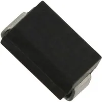
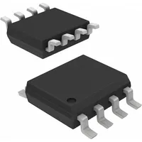
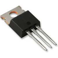
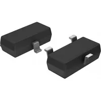
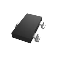
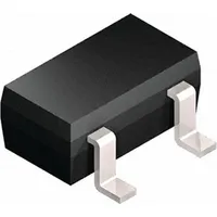
Onsemi BSS138LT3G
|
|
||||
|
|
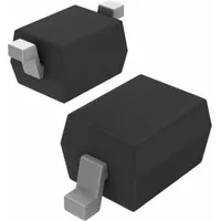
Discover the BSS138LT3G by Onsemi, a high-quality small signal field effect transistor that offers exceptional performance and reliability. As a trusted manufacturer, Onsemi ensures superior craftsmanship and cutting-edge technology in every product they produce. This N-channel transistor, with its single configuration and built-in diode, is perfect for various switching applications. With a maximum drain current of 0.2A and a minimum DS breakdown voltage of 50V, this transistor delivers optimal power and efficiency. Its surface mount capability and gull wing terminal form make it easy to integrate into any design. Experience the value, benefits, and advantages that the BSS138LT3G brings to your projects – choose reliability and performance with Onsemi.
Package Body Material: PLASTIC/EPOXY
Provides durability and protects the internal components of the transistor, ensuring a longer lifespan.
Polarity or Channel Type: N-CHANNEL
Allows for efficient current flow and control in the specified direction, enhancing the performance of the transistor.
Transistor Application: SWITCHING
Suitable for switching applications, making it versatile and ideal for various electronic circuits.
Minimum DS Breakdown Voltage: 50 V
With a high breakdown voltage, this transistor can handle higher voltages without malfunctioning or breaking down.
Operating Mode: ENHANCEMENT MODE
Operates in enhancement mode, which allows for efficient switching and control of the transistor.
Maximum Drain Current (ID): 0.2 A
Capable of handling a maximum drain current of 0.2 A, suitable for various low power applications.
Maximum Drain-Source On Resistance: 3.5 ohm
Low drain-source on resistance ensures minimal power loss and efficient performance of the transistor.
Maximum Operating Temperature: 150 °C
With a high operating temperature range, this transistor can withstand heat and operate reliably in various environments.
| Package Body Material: | PLASTIC/EPOXY |
| Maximum Time At Peak Reflow Temperature (s): | 40 |
| Configuration: | SINGLE WITH BUILT-IN DIODE |
| Transistor Element Material: | SILICON |
| Field Effect Transistor Technology: | METAL-OXIDE SEMICONDUCTOR |
| Transistor Application: | SWITCHING |
| Maximum Drain Current (ID): | .2 A |
| Sub-Category: | FET General Purpose Powers |
| Surface Mount: | YES |
| Terminal Finish: | Matte Tin (Sn) - annealed |
| No. of Terminals: | 3 |
| Maximum Power Dissipation (Abs): | .225 W |
| Terminal Position: | DUAL |
| Package Style (Meter): | SMALL OUTLINE |
| JESD-30 Code: | R-PDSO-G3 |
| No. of Elements: | 1 |
| Package Shape: | RECTANGULAR |
| Terminal Form: | GULL WING |
| Operating Mode: | ENHANCEMENT MODE |
| Maximum Operating Temperature: | 150 Cel |
| Maximum Drain-Source On Resistance: | 3.5 ohm |
| Moisture Sensitivity Level (MSL): | 1 |
| Other Names: | 2832-BSS138LT3GTR<br>2156-BSS138LT3G-OS<br>BSS138LT3GOSDKR<br>BSS138LT3GOSTR<br>BSS138LT3G-ND<br>ONSONSBSS138LT3G<br>BSS138LT3GOSCT<br>=BSS138LT3GOSCT-ND |
| Maximum Feedback Capacitance (Crss): | 5 pF |
| JEDEC-95 Code: | TO-236 |
| Polarity or Channel Type: | N-CHANNEL |
| JESD-609 Code: | e3 |
| Minimum Operating Temperature: | -55 Cel |
| Minimum DS Breakdown Voltage: | 50 V |
| Qualification: | Not Qualified |
| Maximum Drain Current (Abs) (ID): | .2 A |
| Peak Reflow Temperature (C): | 260 |
| ECCN | EAR99 |
| ECCN Governance | EAR |


