Onsemi FDV304P
|
|
||||
|
|
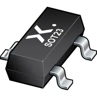
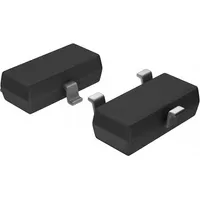
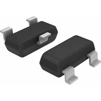
Discover the FDV304P by Onsemi, a top-quality P-CHANNEL Small Signal Field Effect Transistor perfect for switching applications. With a single configuration and built-in diode, this transistor offers enhanced performance and reliability. The FDV304P's metal-oxide semiconductor technology ensures efficient operation while its compact design and surface mount capability make it versatile for various electronic projects. Trust in Onsemi's reputation for excellence and choose the FDV304P for your next application to experience superior quality and value.
Package Body Material: PLASTIC/EPOXY
This material provides good durability and protection for the transistor, making it reliable for various applications.
Polarity or Channel Type: P-CHANNEL
P-channel transistors are known for their low on-resistance and high current capability, making this transistor suitable for switching applications.
Configuration: SINGLE WITH BUILT-IN DIODE
The built-in diode allows for easy implementation of circuit protection mechanisms and can also be used in rectification circuits.
Transistor Application: SWITCHING
Specifically designed for switching applications, this transistor offers fast operation and efficient performance in such scenarios.
Surface Mount: YES
Surface mount technology enables easy and compact integration of the transistor onto circuit boards, saving space and simplifying assembly processes.
Minimum DS Breakdown Voltage: 25 V
With a minimum breakdown voltage of 25V, this transistor can handle higher voltages without experiencing breakdown, ensuring reliable operation.
Maximum Drain Current (ID): 0.46 A
Capable of handling a maximum drain current of 0.46A, this transistor is suitable for applications requiring moderate current levels.
Maximum Power Dissipation (Abs): 0.35 W
With a maximum power dissipation of 0.35W, this transistor can effectively dissipate heat generated during operation, preventing overheating.
Maximum Operating Temperature: 150 °C
The high operating temperature range of up to 150°C allows this transistor to withstand elevated temperatures in various environments.
Minimum Operating Temperature: -55 °C
Capable of operating in extremely low temperatures down to -55°C, making it suitable for a wide range of temperature conditions.
| Package Body Material: | PLASTIC/EPOXY |
| Maximum Time At Peak Reflow Temperature (s): | 30 |
| Configuration: | SINGLE WITH BUILT-IN DIODE |
| Transistor Element Material: | SILICON |
| Field Effect Transistor Technology: | METAL-OXIDE SEMICONDUCTOR |
| Transistor Application: | SWITCHING |
| Maximum Drain Current (ID): | .46 A |
| Sub-Category: | Other Transistors |
| Surface Mount: | YES |
| Terminal Finish: | MATTE TIN |
| No. of Terminals: | 3 |
| Maximum Power Dissipation (Abs): | .35 W |
| Terminal Position: | DUAL |
| Package Style (Meter): | SMALL OUTLINE |
| JESD-30 Code: | R-PDSO-G3 |
| No. of Elements: | 1 |
| Package Shape: | RECTANGULAR |
| Terminal Form: | GULL WING |
| Operating Mode: | ENHANCEMENT MODE |
| Maximum Operating Temperature: | 150 Cel |
| Maximum Power Dissipation Ambient: | .35 W |
| Maximum Drain-Source On Resistance: | 1.1 ohm |
| Moisture Sensitivity Level (MSL): | 1 |
| Maximum Feedback Capacitance (Crss): | 10 pF |
| JEDEC-95 Code: | TO-236 |
| Polarity or Channel Type: | P-CHANNEL |
| JESD-609 Code: | e3 |
| Minimum Operating Temperature: | -55 Cel |
| Minimum DS Breakdown Voltage: | 25 V |
| Qualification: | Not Qualified |
| Maximum Drain Current (Abs) (ID): | .46 A |
| Peak Reflow Temperature (C): | 260 |
| ECCN | EAR99 |
| ECCN Governance | EAR |
| HTS | 8541.21.00.95 |
| SB | 8541.21.00.80 |


